A control sequence is a sequence of control signals being sent out to various modules on subsequent clock cycles to implement a specific opcode. This chapter will go through each of the control sequences that implement the BF instruction set, including supporting instructions. All sequences have been summarized in Table 15 for quick reference (Appendix Microcode Table).
Binary Format
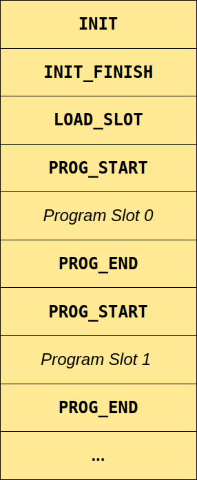
In Section Hardware Overview, it was mentioned that the BF program is stored in ROM as a series of opcodes, each of which corresponds one-to-one to a BF command. However, the system needs to perform some additional non-BF actions to prepare itself for execution. For one, the data-tape is assumed to be zero-initialized; a freshly powered-on SRAM chip will contain random garbage, so we need to take care of that before the first BF command is executed. Moreover, the system is designed to accept a ROM chip containing multiple programs for convenience. This means that before blindly running the first program, there must exist some mechanism that looks for the index corresponding to the program the user is intending to run. To account for these issues, the binary format on the EEPROM expected by the system is as listed below. The bfasm utility was designed to translate any canonical BF source to the corresponding opcodes and dresses them with the necessary housekeeping instructions. The control sequences that implement the initialization and bootloading steps are further discussed in Section Initialization and Bootloading.
One or more INIT instructions to (partially) initialize the data-tape.
One INIT_FINISH instruction to return the data pointer to the start of the data section. This instruction also signals to the IO module that the system has been fully initialized.
One LOAD_SLOT instruction. The program index is supplied to the bus by the IO module and used to move the IP to the start of the corresponding program.
A sequence of BF programs, each preceded by a PROG_START instruction and ended by a PROG_END instruction. The PROG_START instruction serves as a barrier between programs and is used to skip over programs in order to find the correct program to run. PROG_END simply halts the clock and lights up an LED to indicate successful termination of the program.
Instruction Decoding
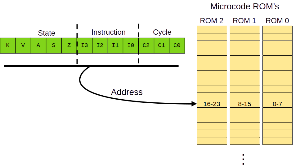
By setting the control signals as described in Chapter Synapse-191 Architecture appropriately, modules can work together to perform each of the BF and supporting instructions. The Control Unit implements this as a lookup-table in 3 ROM chips, where the instruction taken from program ROM (4 bits), flags (5 bits) and cycle counter (3 bits) act as an address into this table (Figure 7). Given that the CU has to be able to supply a total of 24 different control signals, three 8-bit EEPROM chips have been used to store the microcode lookup-table for a maximum of 24 signals (all of them used). More details on the implementation can be found in Section Control Unit.
No simultaneous INC/DEC signals
It is important to note that, because of the choice of driving all of the (counting) registers with a common interface (the Register Driver, see Section Register Driver), only one register can be driven per clock cycle. In other words, the INC and DEC signals can be applied to only one register at a time.
Cycle 0: Instruction Fetch
The first cycle of most instructions is identical3: A, V, S and Z are loaded into the FB register and the current instruction (pointed to by IP) is loaded from program ROM into the instruction register (I). This provides the CU with all the necessary information to determine the control signals for cycle 1: LD_FBI.
Modifying Data: + and -
PLUS
The sequence of instructions necessary to execute a + command depends on the state of the system. Three different scenarios have to be taken into account:
(A = 0, S = 0) - If the A-flag (address-change-flag) is not set, the value in D already corresponds to the value currently pointed to by the DP and no synchronization has to be performed. In that case, its INC signal is immediately asserted to the D register in order for it to increment on the next clock pulse. Referring to Table 1, we see only RS0 has to be asserted in conjunction with the INC signal to increment D (register address 0b001). The V-flag must also be set in order to indicate that the value in D has been changed: this is done by asserting the SET_V signal to FA and latching in the value using the LD(FA) signal.
Now that the value has been incremented and the corresponding flag has been set, the IP is incremented using the register-driver on cycle 2. The cycle reset signal is asserted at the same time.
INC, RS0, SET_V, LD_FA
INC, RS2, CR
(A = 1, S = 0) - However, when the A-flag was set, this means that the address has recently changed and the value inside D does not correspond to the value pointed to by the DP in RAM. We therefore need to fetch the current value from RAM by enabling the DP register on cycle 1, enabling the RAM to output its content on the data bus and loading the resulting value into D. From here on, the control signals are identical to those described above in the case where A was not set.
EN(DP), OE_RAM, LD(D)
INC, RS0, SET_V, LD_FA
INC, RS2, CR
(S = 1) - None of the actions above need to be performed when the S-flag is set, which means that we’re in the process of skipping a loop-block. In this case, we ignore the command and increment the IP immediately and reset the cycle counter: INC, RS2, CR.
MINUS
The control signals necessary to perform the - command are similar to those of the + command, the only difference being the DEC signal to perform a subtraction rather than addition.
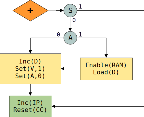
+ command. The diagram for the - command is equivalent (using Dec rather than Inc).Moving the Pointer: < and >
RIGHT
Moving the data pointer one cell to the right requires instructions similar to those of the PLUS instruction, the difference being that we increment the DP register rather than the D register. Similarly, we consider three different scenarios, branching on the V-flag instead of the A-flag:
(V = 0, S = 0) - If the V-flag is not set, it means that the value we point to hasn’t changed and we don’t need to care about synchronization. The DP (register address 010) is incremented immediately and the A-flag is set to indicate we changed the address and are now out of sync. In the second cycle, we move to the next instruction and reset the cycle counter.
INC, RS1, SET_A, LD_FA
INC, RS2, CR
(V = 1, S = 0) - In the case that V was set during one of the previous instructions, we need to write the updated value (present in the D-register) back to RAM before moving the pointer. This is achieved by enabling the value in D onto the data bus and setting the RAM module to write-mode. Furthermore, the V-flag needs to be cleared. This is achieved by loading FA without setting any signals; this will effectively reset both A and V back to zero.
Now that the RAM contains the updated value, it is safe to move the DP to the next cell. The control sequence to do this is identical to the sequence described in the (V = 0)-scenario.
EN_D, WE_RAM, LD_FA
INC, RS1, SET_A, LD_FA
INC, RS2, CR
(S = 1) - None of the actions above need to be performed when the S-flag is set, which means that we’re in the process of skipping a loop-block. In this case, we ignore the command and increment the IP immediately and reset the cycle counter.
INC, RS2, CR
LEFT
The control signals necessary to perform the < command are similar to those of the > command, the only difference being the DEC signal to perform a subtraction rather than addition.
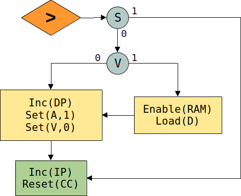
> command. The diagram for the < command is equivalent (using Dec rather than Inc).Conditional Jumping: [ and ]
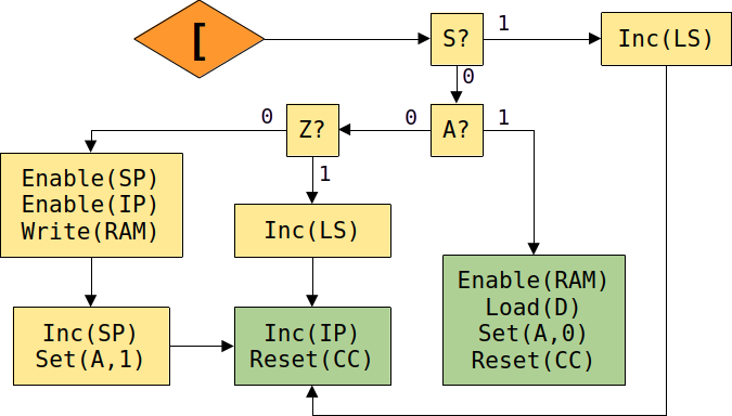
These are by far the most complicated instructions and require lots of additional logic. Because the BF instruction set lacks a JMP instruction where some argument holds the destination address, the computer has to store the address of the opening [ command in case it needs to loop back when the time comes. When a loop is skipped, the LS (Loop Skip) register is used to determine when execution should resume. This leads to multiple scenarios depending on the state of A, Z and S.
LOOP_START
(A = 0, Z = 1, S = 0) - In the first scenario, where A is not set (the D-register is up-to-date) and the Z-flag is set, we can immediately conclude that this loop should be skipped. Hence, the LS-register is incremented and the next instruction is loaded (to be ignored until the LS-register becomes 0 again). Since LS is addressed by the register driver at address 101, both RS0 and RS2 need to be asserted to the register driver. In the second cycle, the IP is incremented and the cycle-counter is reset to move to the next instruction.
INC, RS0, RS2
INC, RS2, CR
Note that these instructions could not take place in the same cycle due to the limitation of the register driver, which can only increment one register per cycle.
(A = 0, Z = 0, S = 0) - In the second scenario, the A-flag is still not set but the Z-flag for the D-register is not set either, meaning that control should enter the loop (the current value is nonzero). It takes 3 cycles to do so: increment the stack-pointer (cycle 1), write the current IP to this address on the stack by enabling it (cycle 2) and move to the next instruction (cycle 3). The corresponding control sequences are therefore:
INC, RS0, RS1
WE_RAM, EN_SP, EN_IP
INC, RS2, CR
(A = 1, S = 0) - In the third scenario the A-flag is set, which means that we should first load the current value from RAM into the D-register (cycle 1) and reset the A-flag. The cycle count is immediately reset to 0 without incrementing the instruction pointer. This means the same instruction is reloaded with updated flags on the next iteration, putting the system into either one of the states above (either scenario 1 or 2, depending on the value of Z).
OE_RAM, LD_D, LD_FA, CR
(S = 1) - In the final scenario, we are in the process of skipping code, indicated by the S-flag (S = 1). In this case, we have encountered a nested loop that needs to be skipped over, so we increment the LS register once more to account for another pair of nested
[]brackets (cycle 1) and then continue to the next instruction (cycle 2). The control sequences are therefore identical to those in the first scenario:INC, RS0, RS2
INC, RS2, CR
LOOP_END
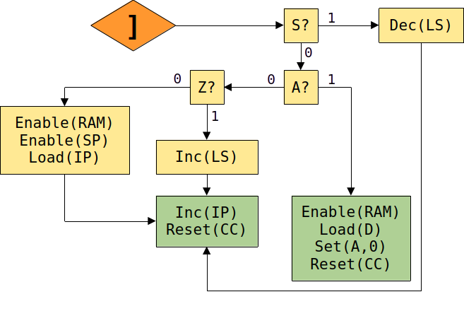
(A = 0, Z = 1, S = 0) - In the first scenario, which takes 2 cycles to execute, there is a known (synchronized) zero in the D-register (A = 0). This means we can immediately choose to exit the loop. To do so, the stack-pointer is decremented (cycle 1) to point at the previous value on the stack. In cycle 2, the IP is incremented as usual.
DEC, RS0, RS1
INC, RS2, CR
(A = 0, Z = 0, S = 0) - In the second scenario, there is a known nonzero value in D. This means we must loop back to the IP-value stored on the top of the stack. This value is loaded into the IP-register by enabling the SP and RAM and setting the LD signal for the IP-register (cycle 1). In the second cycle, this new IP (pointing to a
[) is incremented to re-enter the loop.EN_SP, OE_RAM, LD_IP
INC, RS2, CR
(A = 1, S = 0) - In the third scenario, the contents of D are not yet synchronized with the RAM, so we first need to load it in. After loading the value into D, the flags and cycle counter are reset to put the system back into one of the previously defined states.
OE_RAM, LD_D, LD_FA, CR
(S = 1) - Finally, when already in the process of skipping a loop, the LS register is decremented before moving to the next instruction by resetting the cycle counter and incrementing the IP.
DEC, RS0, RS2
INC, RS2, CR
Output: .
Handshake
Due to the asynchronous nature of the output peripheral, it is necessary to enter into a handshake protocol whenever a byte is put on the bus for display. In this protocol, the K-flag is used to communicate between the CPU and the IO module: it is set by the IO module to indicate that it has read the data from the bus, and reset by the CU to indicate that the handshake has been received and completed. The global step-by-step process is described below. The control sequences (on the side of the CU) that implement these steps follow after. Section IO Module and the code in Appendix IO Module ISR show how the IO Module’s side is implemented.
First, the data is loaded into D if not already present (A=1). The CU then asserts the EN_OUT signal and enables D such that its contents appear on the data bus. It will keep EN_OUT high and keep the data asserted onto the data bus for as long as necessary, as indicated by the K-flag.
The output module notices the EN_OUT signal and reads the value from the bus. When done, it sets the K-flag.
When K is seen to go high, the bus is deasserted, K is reset and the transaction has finished.
Implementation
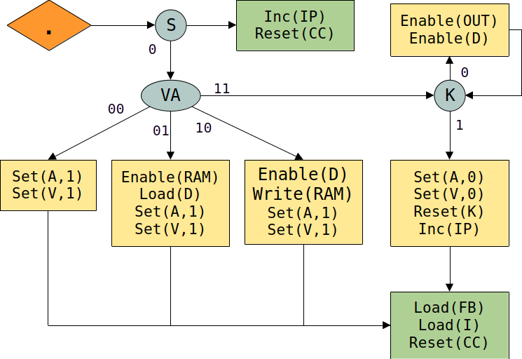
When the OUT instruction hits its first cycle, it will first synchronize D with RAM if the A-flag or V-flag is set. This is necessary because these flags are then both set to 1 to indicate a wait state; synchronizing D allows these flags to both be safely reset when the instruction has finished. In cycle 2, A and V are latched into FB and the CC is reset, in order for the microcode to branch into the wait loop on the next cycle 0. Now that the system is back in cycle 0 with both A and V set, the system goes into a busy loop. The EN_OUT and EN_D signals are continuously asserted for as long as the K-flag is still low; an immediate cycle reset leaves the system in cycle 0. All other commands reload the flags and instruction in cycle 0; to maintain stable data on the bus without interruptions (due to resetting to the default cycle 0), we need the special A=V=1 state to encode this situation. When K finally goes high (K does not have to be latched, so its current value is always available), cycle 0 branches to a different sequence, where the A, V and K flags are cleared and the IP is incremented to move to the next instruction.
(A = 0, V = 0) - No need to synchronize; go into wait-state by setting A and V to 1. Latch these in FB immediately to make them available on the next cycle 0.
SET_A, SET_V, LD_FA
LD_FBI, CR
(A = 0, V = 1) - Synchronize D to RAM and go into the wait-state like before.
SET_A, SET_V, LD_FA, EN_D, WE_RAM
LD_FBI, CR
(A = 1, V = 0) - Synchronize RAM to D and go into the wait-state like before.
SET_A, SET_V, LD_FA, LD_D, OE_RAM
LD_FBI, CR
(A = 1, V = 1, K = 0) - Still waiting for K to go high; keep the data asserted and reset the cycle counter.
EN_OUT, EN_D, CR
(A = 1, V = 1, K = 1) - K has gone high; break out of the wait-state by clearing A and V (loading FA without asserting any signals) and move to the next instruction.
LD_FA, CLR_K, INC, RS2
LD_FBI, CR
Input: ,
Handshake
Similar to the output command, the input command implements a handshake protocol to make sure that the data bus is claimed by the input device for the exact right amount of time, in order for the system to reliably read its contents. This happens using the same K-flag that was used in the output handshake.
The CU asserts the EN_IN signal and will keep this control line asserted until K is set by the IO module, indicating that the data is ready.
The input module notices EN_IN, waits until the keyboard buffer contains a value and puts this on the bus, then it sets K.
When K is seen to go high, the value on the bus is loaded into D and K is cleared to complete the handshake.
Implementation
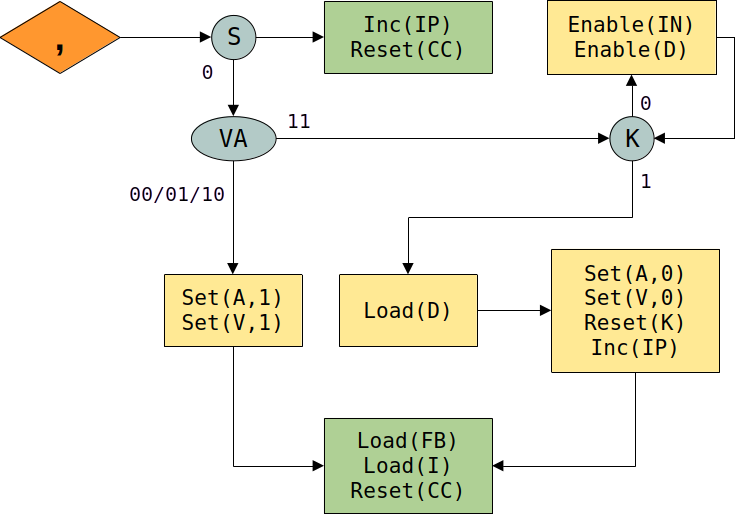
The microcode for the sequences described above is very similar to that of the OUT instruction. Again, the wait state is encoded by setting A and V to 1, allowing the system to spin in cycle 0 while K is not yet set by the IO module. When K goes high, the data on the bus is latched into D, the A and K flags are cleared, V is set and the next instruction is reloaded. As was the case with the OUT instruction, we need an explicit LD_FBI before resetting the CC to compensate for the fact that the flags already have to be up to date when cycle 0 loads in order to implement the busy loop (all other commands refresh the flags in cycle 0). In this case, there is no need to synchronize D and RAM before setting the flags to the wait state. Since we expect a new value to be read into D as a result of this instruction, the V-flag should be set and the A-flag should be reset regardless of the state of the computer on entering this instruction.
(A = 0, V = 0) - Go into wait-state.
SET_A, SET_V, LD_FA
(A = 0, V = 1) - Go into wait-state.
SET_A, SET_V, LD_FA
(A = 1, V = 0) - Go into wait-state.
SET_A, SET_V, LD_FA
(A = 1, V = 1, K = 0) - Still waiting for K to go high; keep enable signal asserted and reset the cycle counter.
EN_IN, CR
(A = 1, V = 1, K = 1) - K has gone high; load the data, break out of the wait-loop by setting V and resetting A, clear K and move to the next instruction.
LD_D
SET_V, LD_FA, CLR_K, INC, RS2
LD_FBI, CR
Input Modes
The input peripheral (probably) manages an internal buffer to serve subsequent bytes to the system, which might be empty when the request for input arrives. When this happens, it is up to the peripheral to decide upon one of two options:
Wait for the buffer to contain data. Only then set the K-flag (buffered mode).
Assert zeros to the bus and set the K-flag immediately (immediate mode).
In our implementation of the IO-module (see IO Module), both modes are supported and can be selected from the options menu.
Initialization and Bootloading
In Section Binary Format a general overview of the contents of the program ROM was given. Before running the program, two main steps have to be taken: initialize the data-tape to zero and jump to the correct program (the EEPROM can contain multiple programs). These two steps are implemented using the INIT, INIT_FINISH, LOAD_SLOT and PROG_START opcodes.
INIT
In any BF program it is assumed that all memory is zero-initialized. In practice, SRAM-modules will contain random values at startup, so the assembler must add a preamble to the main code in order to initialize the RAM (or at least part of it) to 0. While this could in principle be implemented in terms of canonical BF commands (initializing one cell at a time using a sequence of [-] commands) it is much faster to write a bunch of known zeroes directly to RAM. This is the purpose of the INIT instruction: for each INIT instruction, a contiguous chunk of 256 memory-cells will be zero-initialized. Since it is guaranteed that the D register contains a zero after reset, this value can be directly written into RAM on the first cycle of INIT. The LS and DP registers are incremented during the first and second cycles, respectively. DP is incremented to move through the memory-space whereas LS is incremented in order to count to 256, at which point the S-flag will go low again due to the LS register overflowing back to 0. If more memory needs to be initialized, the assembler can simply concatenate multiple INIT instructions.
EN_D, WE_RAM, INC, RS0, RS2 (write a zero to the current cell and increment the LS register)
LD_FBI, INC, RS1 (increment the DP register)
Depending on whether the LS-register wrapped around (256 cells initialized), either move to the next cell or finalize by incrementing the IP and resetting the cycle-counter.
(S = 0) - INC, RS2, CR
(S = 1) - CR
After the appropriate number of INIT instructions have been executed, the INIT_FINISH instruction (see below) must be called in order for the DP to return to the start of the memory (0x0100).
INIT_FINISH
The INIT_FINISH opcode is designed to do two things: it resets the DP to the start of the data section (0x0100) and it resets the K-flag. The former is necessary after initialization, which leaves the DP at whatever the last cell was that was initialized, and is achieved by asserting the CLR_DP signal. The latter will tell the IO module that initialization is finished (the IO module sets the K-flag at boot). The IO module will respond to this by taking ownership of the bus and writing the program slot to it. The LOAD_SLOT instruction (which always immediately follows the INIT_FINISH instruction) will use this value to skip to the desired program.
LOAD_SLOT
As described above, the IO module will have put the program slot (set by the user through the IO menu) onto the bus by the time the LOAD_SLOT opcode is executed. To avoid race conditions, we wait for the K-flag to go high, meaning that the data is ready to be read from the bus. Once it does, we leverage the existing loop-skip mechanism to skip over entire programs rather than loops inside a program. First, we load the program index from the bus into D and increment the LS register to go into skip-mode (LS now has value 1 so the S-flag goes high). We then clear the K-flag to let the IO module know that it should disable its outputs. Since the system is in skip now, every normal BF instruction will be skipped entirely.
LD_D, INC, RS0, RS2 (load slot index and increment LS)
CLR_K, INC, RS2 (clear the K-flag and increment IP)
PROG_START
The only opcode that performs non-trivial actions while the system is in skip-mode (initiated by incrementing LS as described above) is PROG_START. It checks the value in D, which was initially populated with the index of the desired program (0, 1, 2, ...), to see if the IP has arrived at the correct location: if the Z-flag is set (D = 0), we exit skip-mode and enter the program following the current PROG_START instruction. If the Z-flag is not set (), we decrement D and keep scanning. In other words, D is decremented on each PROG_START until it hits zero, i.e. the selected program slot has been reached.
(S = 1, Z = 0) - D still holds a nonzero value. Decrement D and continue in skip-mode:
DEC, RS0
INC, RS2, CR
(S = 1, Z = 1) - D is zero. Exit skip-mode (decrement LS) to run subsequent code.
DEC, RS0, RS2
INC, RS2, CR
Note that, while skipping over entire programs, the LOOP_START and LOOP_END instructions will still have the effect of incrementing and decrementing LS. However, since LS starts out at 1 and programs are guaranteed to contain matching brackets (enforced by the assembler), it is guaranteed to contain the value 1 when the entire program is skipped over (it will have undergone an equal number of increment and decrement operations). Decrementing it a final time (Cycle 1 of Scenario 2) is therefore guaranteed to bring it back to 0, disabling the S-flag.
Convenience Opcodes
While all of the opcodes above would be sufficient to run any BF program, it is still convenient to be able to halt the clock, indicate that an error occurred or tell the user that the end of the program was reached successfully. Furthermore, the common extension Random Brainfuck [3] is implemented as an additional instruction (RAND) that acts just like the IN instruction, except now a random number appears on the bus rather than user input (handled by the IO module as well). All non-BF opcodes are listed and described below.
NOP
The NOP instruction does nothing. It simply increments the IP and resets the cycle count to move to the next instruction.
INC, RS2, CR
HALT
The HALT instruction halts the clock and (temporarily) stops the program by asserting the HLT signal. The assembler will place a HALT instruction before the first and after the final instruction of each program. The former allows the user to manually start the program after the system has been fully set up and the latter prevents the program from continuing into invalid memory after it has executed its final command. Furthermore, the assembler can (optionally) interpret an exclamation mark (!) as a HALT in the BF-code to set breakpoints for debugging. When the system is resumed and cycle 2 of the HALT instruction is reached, the IP is incremented as usual in the final cycle of any instruction.
HLT
INC, RS2, CR
PROG_END
The PROG_END instruction is basically a HALT instruction that also lights up an LED by asserting the END signal. This lets the user know that the end of the program was reached gracefully. Unlike the HALT instruction, no Cycle 2 has been defined. Trying to resume the clock after a PROG_END was reached will therefore result in the ERR signal being raised (see below).
HLT, END
Error States
There is no opcode to put the system into an error state explicitly. However, every address in the microcode table that corresponds to an unspecified state contains the HLT and ERR signals to stop the clock and light up the error LED. The system should never go into such a state, no matter what errors the BF program contains. However, it proved invaluable during testing, when the microcode sequences themselves still contained mistakes.