Hardware Overview
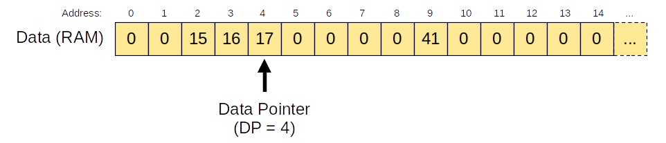
A true BISC implementation is a direct representation of the abstract BF machine described in Section Brainfuck, consisting of an array of memory-cells together with a pointer pointing to one of these cells. The pointer can move along the array while modifying its contents one step at a time. Figure 3 illustrates an example intermediate state of such a system. Consider the BF program “>>>>>+.”, applied to the initial conditions shown in the example. The pointer would take 5 steps to the right, landing on cell 9 which contains the number 41. It will then increment and output this value, displaying 42 on the screen (assuming a screen of some sort is used as the output device and it is displaying numbers directly rather than interpreting them as ASCII).
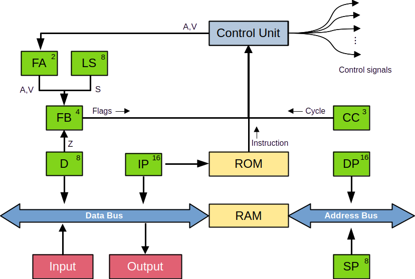
In a physical system, the data-tape would be a large memory space in RAM and the data pointer is a register that holds a value representing an address within that space. The pointer is moved by simply changing the value stored in the data pointer register. Modifying values in regular systems happens inside the ALU (Arithmetic and Logic Unit), which is capable of addition, subtraction, multiplication and many more mathematical and logical operations. No full-blown ALU is needed in a BISC implementation because of the simplicity of the modifying operations: values only need to be incremented or decremented (this goes for both the data pointer and the data itself), which can be done directly at the register level when up/down binary counters like the 74LS193 integrated circuit are used. The program (a sequence of BF instructions) is stored in Read-Only Memory (ROM), whereas the data is stored in Random Access Memory (RAM). Instructions (4-bit) are fed from ROM into a control unit (CU) together with a set of flags (see Flags) that encode the state of the machine. Depending on the state and current instruction, the CU sets the appropriate control signals for each of the modules (memory, registers and I/O) in order for the system to perform the appropriate actions. Table Overview of the modules that make up the physical BISC implementation. lists the components of this BISC implementation, whereas Figure 4 shows the (conceptual) connections between those modules. In the sections below, each of these connections will be clarified further. The actual implementation on the logic/hardware level is described in Chapter Hardware Implementation.
Flags
The state of the system is encoded using five flags: K, V, A, S, and Z. These flags were introduced to simplify control logic and enable performance optimizations during execution. Each flag serves a specific purpose, as explained below:
K-Flag
The K-flag is used for communication between the system and the IO Module, which run asynchronously. The flag is set by the IO Module and reset by the system to let each other know when certain data transactions have been completed.
A-Flag
The A-flag is set when the value in the DP register was modified, i.e. when the data pointer has been shifted to a new cell. This is an architectural optimization to minimize the number of reads from and writes to RAM. Consider a long sequence of + or - instructions, which are very common in BF programs. A naive implementation of, for example, the + instruction, would consist of 3 steps: read the current value from RAM into D, increment the value in D, write the result back to RAM. However, when it is known that the data pointer has not been changed, we can keep operating on the copy in D. Only when the address has been changed (A was set), should we load the new value into D before modifying it.
V-Flag
The V-flag allows for another optimization, similar to that of the A-flag. Whenever the value in the D register has been modified, the V-flag is set. When the DP is about to change its value, through the < and > commands, the V-flag is checked. If set, we store the modified value back into RAM before moving the pointer. If not, the value hasn’t changed and does not need to be synchronized into RAM. The number of cycles to complete long sequences of pointer move-commands is decreased substantially using this approach.
S-Flag
The S-flag is used to skip over blocks of code, primarily when skipping over loop-blocks. It is set when a loop should not be entered, causing all following commands to be ignored until the matching closing bracket is reached. Similarly, it is used at boot to skip over entire programs until the selected program is reached (when multiple BF programs have been written to the same program ROM).
Z-Flag
The Z-flag is set by the D register whenever it contains the value zero. This allows control-flow to branch on the value of the current cell, allowing for the implementation of loops.
Performance Gains
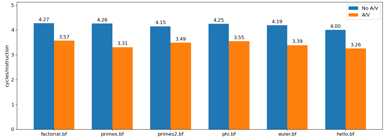
The number of cycles saved from using the A and V flags depends on the program that is running; programs with long and frequent sequences of +, -, < or > commands will benefit more than those with fewer or shorter sequences. To investigate the actual impact, a test suite of BF programs was put together and run in an emulator (a modified version of the C example shown in Listing 1). The BF source for each of these programs is shown in Appendix BF Test Suite. The modified interpreter contains a table of the number of cycles necessary to execute each instruction, depending on the aforementioned flags. This allows for a quantitative comparison between the naive implementation (load, modify, store) and the cache-like approach using the A and V flags. The results are shown in Figure 5; a 16 to 22% decrease was observed when using the A and V flags.
Data Pointer Register (DP)
The data-pointer corresponds to the pointer as specified in the BF-language. It points to some value in memory beyond the stack ( 0x0100, see Stack Pointer Register (SP)) and can be either incremented (moved right) or decremented (moved left) using the > and < instructions. Whenever the value pointed to by DP is modified by + or -, it is loaded into the D-register (see Data Register (D)), where it can be modified before being stored back into RAM.
Inputs
The DP should be able to increment and decrement (corresponding to the < and > commands), and should be able to be enabled/disabled because of its connection to the address bus of the RAM (the Stack Pointer (SP; see Stack Pointer Register (SP)) is also connected to this bus). While all other modules have the ability to be reset, the DP is the only register that can be reset (to 0x0100) at runtime. This is necessary during boot, when all the data cells need to be initialized to 0 (see Initialization and Bootloading).
EN - Enable - Assert the stored 16-bit value onto the address bus.
U - Up - Increment the stored value.
D - Down - Decrement the stored value.
R - Reset - Reset the value to 0x0100, the start of the data section of RAM.
Outputs
DP_OUT - 16 bits, asserted onto the address bus when enabled (EN high).
Data Register (D)
The data register holds a representation of the value currently pointed to by the DP and can be incremented and decremented (using the + and - commands). This register provides the Z-flag to signify that its current value is 0. Among other things, this flag can be used to determine whether or not to enter a loop.
Inputs
D_IN - 8 bits - Data inputs, connected to the data bus.
EN - Enable - Assert the stored value onto the data bus.
LD - Load - Load data from the bus into D.
U - Up - Increment the stored value.
D - Down - Decrement the stored value.
Outputs
D_OUT - 8 bits - Data outputs, connected to the data bus.
SET_Z - Set Zero Flag - High when the register stores a zero, connected to FB.
Instruction Pointer Register (IP)
The IP Register stores the instruction pointer (16-bits), which keeps track of the instruction that is currently being executed. It points to a certain address in ROM (which stores the program) and is usually incremented after each instruction has finished executing, in order to move to the next instruction. However, when the processor encounters the [-instruction (and a loop is entered), its value is stored in RAM at the location pointed to by the stack pointer (SP, see Stack Pointer Register (SP)). When the matching ]-instruction is encountered, this value can be loaded back into the IP in order to jump back to the start of the loop if needed.
Inputs
IP_IN - 16 bits - Data inputs, connected to the data bus.
EN - Enable - Assert the stored value onto the data bus.
LD - Load - Load data from the bus into IP.
U - Up - Increment the stored value.
Outputs
IP_OUT - 16 bits - Data outputs, connected to the data bus and the address inputs of program-ROM;
Stack Pointer Register (SP)
The stack is the first part of RAM (addresses 0x0000 - 0x00FF) and is reserved to keep track of addresses in ROM that might need to be jumped to when flow encounters a loop-end instruction (]). The stack-pointer (SP) points to an address in this space; it is incremented whenever a new jump-address is pushed to the stack and decremented whenever an address is popped off the stack. In this implementation, the SP is an 8-bit value, which means that at most 256 different values can be stored onto the stack before the SP overflows (wraps around back to 0) and starts overwriting previous values. This would happen if a BF program was loaded that has more than 256 nested []-pairs (and each of those loops is entered). Although possible, it is very unlikely to happen for the simple programs we intend to run. In Chapter Runtime Results, where the required stack size is measured for a suite of test programs, this is confirmed; the largest value found for any required stack size in these programs was only 17, leaving plenty of space for even more complex programs.
Inputs
EN - Enable - Assert the stack-pointer onto the address-bus.
U - Up - Increment the stack-pointer.
D - Down - Decrement the stack-pointer.
Outputs
SP_OUT - 8 bits - connected to the address bus of RAM.
Loop Skip Register (LS)
The Loop Skip (LS) register is a counter that indicates whether or not we’re in the process of skipping a loop. In BF, a loop ([) is only entered when the value currently pointed to is nonzero. In the case that it is zero, execution resumes beyond its matching loop-end instruction (]). When it is determined that a loop must be skipped (based on the Z-flag provided by the D-register), the LS register is incremented from 0 to 1 and the S-flag is set. This flag will remain set as long as the value in LS is nonzero, indicating that the system is in a skip-state. Subsequent instructions are then skipped until either another (nested) loop-start or a closing loop-end is encountered. On the former, the LS is incremented again while on the latter the LS is decremented. This has the effect that the LS becomes 0 again after the ] that matches the original [ which led to the skip. Normal execution occurs as soon as LS has become 0 again and the S-flag is reset back to 0.
Inputs
U - Up - Increment the stored value.
D - Down - Decrement the stored value.
Outputs
SET_S - Skip flag - set when its value is nonzero, connected to FB.
Flag Registers (FA and FB)
FA
The first flag register (FA) holds two flag values, A and V, which are used to indicate that either the address (A) or value (V) has changed during one of the previous instructions. For instance, if D was incremented (or decremented), the V-flag is set to indicate a change of the value being pointed to: the value in RAM is now outdated. When DP is incremented (or decremented), the A-flag is set to indicate a change of the current address, meaning that the value in D is now outdated. For a more detailed description of the function and application of these flags, refer to Sections Modifying Data: + and - and Moving the Pointer: < and >.
FB
On the zeroth cycle of every instruction, these flags are latched into the FB register together with the Z and S-flags (set by the D and LS registers) for a total of 4 flags. This happens simultaneously with loading the next instruction into the instruction register (I, see Instruction Register (I)) and is not refreshed until loading the next instruction to make sure that the flag-state remains constant throughout the execution of the current instruction.
K-Flag
The previously mentioned K-flag is specific to interactions with the IO-module and is not buffered in either of the flag registers. It is discussed more thoroughly in Sections Output: . and Input: ,.
Inputs
SET_A - Assert the address-change-flag onto FA.
SET_V - Assert the value-change-flag onto FA.
LD(FA) - Load A and V into FA (if set).
LD(FB) - Load A, V (previously buffered in FA), Z and S (from D and LS) into FB.
Outputs
F_OUT - 4 bits - connected to the instruction decoder inside the Control Unit.
Instruction Register (I)
The instruction register I buffers the current instruction pointed to by the IP. The instruction is loaded from program ROM into I at the start of every new instruction (cycle 0), right after IP has been incremented. Its outputs are used as part of the microcode address that goes into the decoder of the CU (see Figure 7 in Chapter Opcodes and Control Sequences).
Inputs
LD(I) - Load the instruction pointed to by IP.
Outputs
I_OUT - 4 bits - connected to the instruction decoder inside the Control Unit.
Register Driver
Rather than having a separate signal for each of the INC/DEC inputs of each register (e.g. INC_D, INC_LS, etc.), a driver module was designed (see Register Driver) to drive registers that support modification of their contents (increment/decrement). In addition to a universal INC/DEC signal, three Register Select (RS) bits are used to index the target register. This approach has two advantages:
It decreases the number of control signals needed;
The logic needed to drive the counting registers (74LS193) only needs to be implemented once.
The driver module accepts 5 control signals: 3 register-select signals (RS0 through RS2), INC and DEC. Using 3 register-select signals, up to 8 () registers can be selected, though only 5 need to be driven by the driver. Table 1 contains an overview of each of the registers and the control signals they support. When all RS-signals are off, no register is selected.
| Register | #Bits | EN | LD | INC | DEC | RS2RS1RS0 |
|---|---|---|---|---|---|---|
| D | 8 | x | x | x | x | 001 |
| DP | 16 | x | x | x | 010 | |
| SP | 8 | x | x | x | 011 | |
| IP | 16 | x | x | x | 100 | |
| LS | 8 | x | x | 101 | ||
| FA | 4 | x | not addressable | |||
| FB | 4 | x | not addressable | |||
| I | 4 | x | not addressable |
Inputs
RS0 - Register Select Bit 0
RS1 - Register Select Bit 1
RS2 - Register Select Bit 2
INC - Increment selected register
DEC - Decrement selected register
Outputs
U - 5 bits - Up signals - Connected to the U input of all registers that support the INC operation.
D - 5 bits - Down-signals - Connected to the D input of all registers that support the DEC operation.
Cycle Counter (CC)
Almost every BF instruction requires multiple cycles to complete. Therefore, in addition to the instruction and state, a cycle counter is used to determine the control signals that should be sent out at each step of the instruction. This cycle counter is implemented as a 3-bit counting register (allowing for at most 8 cycles per instruction) that increments on every clock cycle and sends its output to the control unit. Its only control signal is the clear signal (CLR) which resets the count to 0, in order to fetch the next instruction.
Inputs
CLR - Cycle Reset - Reset the count to 0;
Outputs
CC_OUT - 3 bits - Current value of the register (0–7).
Data Memory (RAM)
RAM is divided into two parts: stack and data. The first 256 bytes (0x0000 - 0x00FF) make up the stack and are indexed by the stack pointer (Stack Pointer Register (SP)). The data (corresponding to the BF tape) is stored at addresses 0x0100 through 0xFFFF and is indexed by the data pointer (Data Pointer Register (DP)). Its address lines are connected to the address bus, which in turn receives its value from either the DP or the SP. Its data lines are bidirectional and are connected to the data bus. When the Write Enable (WE) signal is active, data can be read from the bus and written into RAM. When instead the Output Enable (OE) signal is active, the current value in RAM (determined by the address on the address bus) is asserted onto the data bus.
Inputs
DATA_IN - 16 bits - Input data, connected to the data bus.
ADDR_IN - 16 bits - Address lines, connected to the address bus;
OE - Output Enable - Assert the value stored at the current address onto the data bus;
WE - Write Enable - Write the value on the data bus into the current address.
Outputs
DATA_OUT - 16 bits - Output data, connected to the data bus (same physical lines as DATA_IN).
Program Memory (ROM)
The actual BF instructions are stored in Read-Only-Memory (ROM) and are addressed by the IP (Instruction Pointer Register (IP)). A 4-bit instruction is stored at the address pointed to by the IP. It is sent to the CU where it is used to determine the set of control signals, together with the flags and cycle counter.
Inputs
ADDR_IN - 16 bits - Address lines, connected to the IP.
Outputs
INS_OUT - 4 bits - Instruction data, connected to the CU.
Screen (SCR)
The output module (which is assumed to be a screen) will be attached to the data bus and will display whatever is on the bus when enabled using the EN signal. Because the output is handled asynchronously by some peripheral that will, from the perspective of the CPU, be viewed as a black box, it needs a flag to acknowledge a successful data-transfer. This is done through the K-flag, which is set by the peripheral after reading data from the data bus (this flag is shared with the input device for a similar purpose). The K-flag can only be reset by the CU using the CLR_K signal, indicating that the transfer procedure has been completed.
Inputs
DATA_IN - 8 bits - connected to the data bus.
EN: Enable - Display the contents of the bus. The format of the output (ASCII, hex, etc) may vary depending on the implementation of the output device.
CLR_K - Clears the K-flag - connected to the CU (this signal is shared with the input module, KB; see Keyboard (KB)).
Outputs
None.
Keyboard (KB)
The input device to the computer is assumed to be a keyboard of some sort1 that implements a buffer from which some 8-bit value can be requested. The control unit can assert the enable signal of this device and should then wait until the K-flag is set, at which point the data should be ready to be read from the data bus. It is left up to the implementation of the peripheral to decide what to do when there is nothing in the input buffer (either wait for user input or return 0). The K-flag, which is shared with the output peripheral, is reset to communicate that the data has been transferred and the input device can yield control of the data bus back to the system.
Inputs
EN - Enable - Make the contents of the input buffer available on the data bus.
CLR_K - Clears the K-flag - connected to the CU (this signal is shared with the output module, SCR; see Screen (SCR)).
Outputs
DATA_OUT - 8 bits - Output data, connected to the data bus.
Control Unit
Each of the aforementioned components/modules has one or more control inputs that determine what happens on the next clock cycle. For example, some register-modules can be told to load a value from their input, increment or decrement the currently stored value, or do nothing at all. It is the Control Unit (CU) that supplies the appropriate control signals to each of the modules before the next clock pulse occurs, depending on the current instruction and state determined by the flags and cycle counter. The implementation details of how this is done in hardware are discussed in Chapter Hardware Implementation.
Inputs
CC_IN - 3 bits - Cycle counter input lines.
INS_IN - 4 bits - Instruction input lines (from program ROM).
FLAGS_IN - 5 bits - Flag input lines (from FB and K).
Outputs
HLT - Halt Clock
RS0 - Register Select, bit 0
RS1 - Register Select, bit 1
RS2 - Register Select, bit 2
INC - Increment selected register
DEC - Decrement selected register
CLR_DP - Reset DP
EN_SP - Enable SP to address bus 2
OE_RAM - Output Enable RAM
WE_RAM - Write Enable RAM
EN_IN - Enable input (keyboard) to data bus
EN_OUT - Enable output device
SET_V - Set V-flag in FA
SET_A - Set A-flag in FA
LD_FBI - Load FB and I
LD_FA - Load FA
EN_IP - Enable IP
EN_D - Enable D to data bus
LD_D - Load D
LD_IP - Load IP
CLR_CC - Reset Cycle Counter
CLR_K - Clear the K-flag in the IO module
END - Program End Signal
ERR - Error Signal