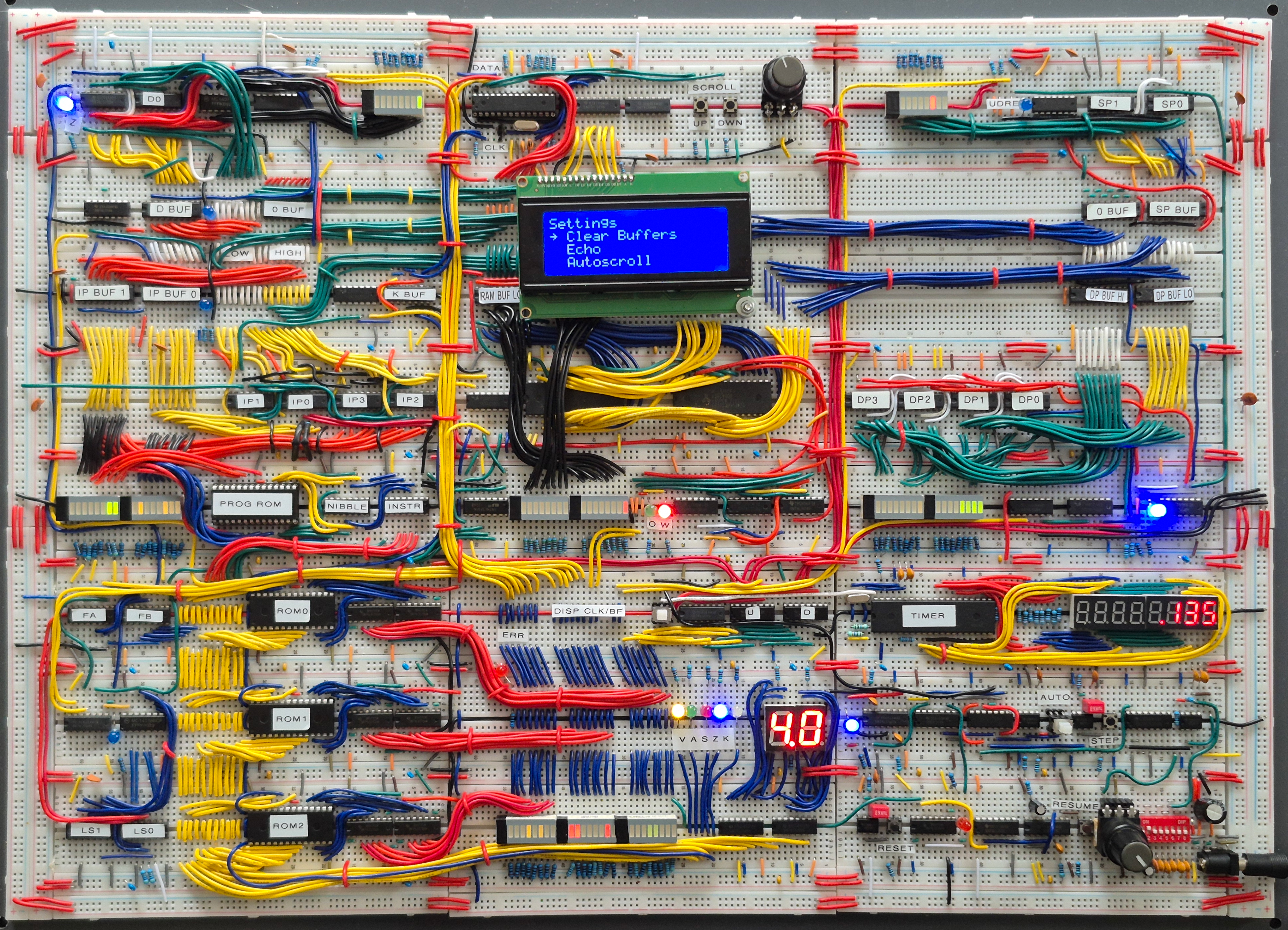
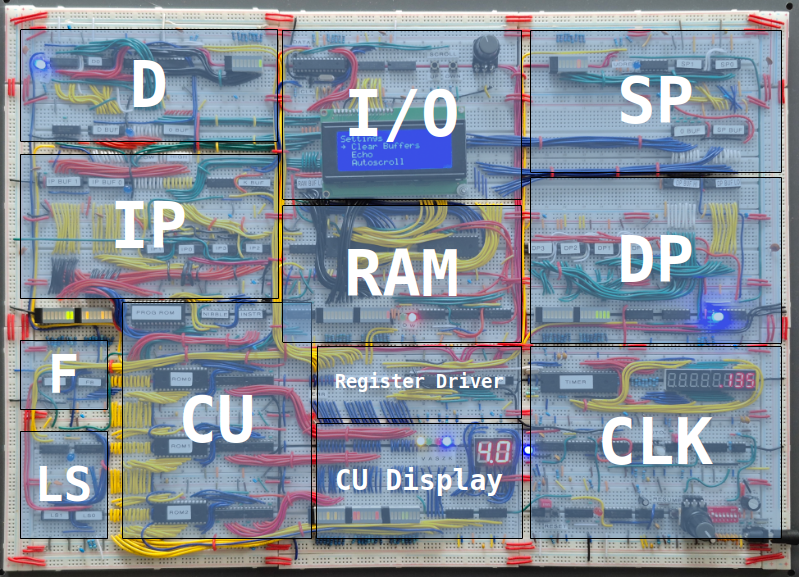
This chapter will discuss the implementation of each module and the way they integrate together to make the computer. Figure 14 shows the computer as it was in February 2025. The overlays shown in Figure 15 show where each of the modules described in the previous chapter is located on the computer. Schematics for each of the modules can be found in Appendix Schematics.
Wiring
Breadboards
The entire system was implemented on 830-hole breadboards. When the project started, relatively cheap breadboards were used, which had segmented power rails. These had to be bridged with jumper wires, but these connections proved somewhat unreliable, introducing subtle points of failure. This is why, at a later stage of the build, we moved to more expensive but more reliable breadboards with continuous power rails.
Wires
Most of the longer wires were cut from spools of either 22AWG or 20AWG wire. While 22AWG proved reliable enough almost all the time, the thicker 20AWG had noticeably stronger connections to the breadboards and has been used mainly to make reliable power and ground connections. Thinner jumper wires have been used for short connections, e.g. connections from ICs’ VCC and GND pins to the power rails. These are very convenient to use—cutting and stripping short wires is a tedious job—but have sometimes been the source of hard-to-identify instabilities that were eventually identified as bad connections to ground, caused by these jumper wires.
Busses
In Ben Eater’s implementation of the 8-bit CPU, power rails cut loose from breadboards were used to build the central bus, which makes it easy for modules to connect to it. Because our system has two busses (8 and 16 bits wide), this would have been impractical to replicate.
Bus Pull-Down
The data bus can be written to by 3 different modules: D, IP and the input device (usually KB). To prevent floating bits at times when none of these devices are active, each of the 8 bus lines is connected to ground through a 1K resistor. Even though the microcode implementation prevents any module from reading from the bus when no other module is enabled, this was done anyway in the spirit of good practice. The 16-bit address lines are guaranteed to be in a valid state since either the DP or the SP has its outputs enabled at any time during execution. Therefore, no pull-down resistors were used on the address bus.
Power
Power is supplied by a 5V, 3A power supply (the system draws around 930mA), connected to power rails that run around the perimeter of the system and in between the breadboards. As many interconnections as possible between different parts of the power rails were made to ensure that all segments of the board receive a stable power supply and connection to ground. At short intervals, 100nF capacitors were placed across the rails to filter high-frequency noise.
Clock and Reset
Many of the modules need a connection to the clock and reset lines, which is why power lines cut loose from spare breadboards were repurposed to function as clock/reset rails that run around the perimeter of the board. This provides easy access to those lines even for modules at the opposite end of the system relative to the clock and reset modules.
LED Indicators
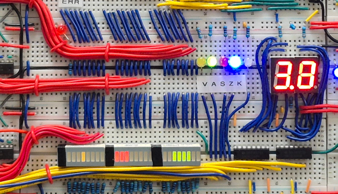
To be able to monitor the state of the machine visually (and for dramatic effect), many LED indicators have been installed across the board. LED bars were used to visualize the register contents and control signals, while single LEDs were used to show the status of flags and enable signals. Each LED is wired in series with a 470 resistor to ground.
Additionally, two 7-segment displays, each driven by a 74LS48, are connected to the instruction register and cycle counter to display the current instruction and cycle as decimal numbers (e.g. 4.2 for cycle 2 of the > instruction, see Assembler: bfasm). Unfortunately, the ’48 does not support values over 9 (no hexadecimal representation) so non-BF opcodes like INIT lead to a blank display.
Clock and Controls
Clock
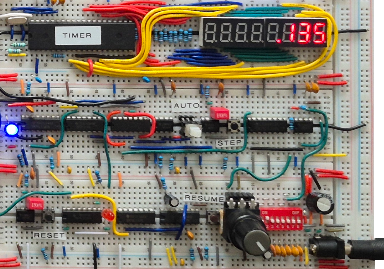
The clock module is located at the bottom right of the computer and is responsible for providing a heartbeat to (most of) the modules. The core design of the clock, based around a 555 timer in astable mode, is taken directly from Ben Eater’s 8-bit computer videos [5]. The output frequency can be set using an array of DIP switches to select the capacitor of an RC circuit for coarse control and a 10K linear potentiometer for fine control. Two additional 555 timers are used to debounce both the pushbutton for the manual clock and the latching pushbutton which acts as a selector between the two modes, as per Ben’s design.
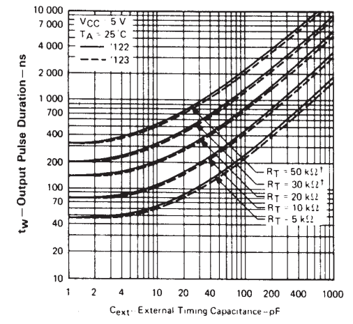
The frequency of the astable 555 is halved by sending it through a JK flip-flop to ensure a perfectly symmetric duty cycle, then fed into a 74LS123 monostable multivibrator to produce two short 200ns pulses: one on the rising edge and another on the falling edge of the output of the flip-flop. The 200ns pulse is generated by connecting a 100pF capacitor and a 5K resistor to the ’123, in accordance with the timing diagram from the datasheet [27], shown in Figure 18.
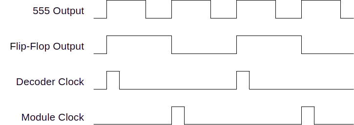
This results in two sets of clean signals at constant intervals. On the first pulse (rising edge of the output of the flip-flop), control signals are loaded from the microcode EEPROMs into a set of registers (74LS173) that buffer these control signals for stability; even when the inputs to the EEPROM address-pins change during execution of an opcode, this will not affect the control signals presented at the modules. The second pulse (generated by the falling edge of the flip-flop) is used as a clock to the modules; this is when the modules execute their command, like loading a value into RAM or incrementing the contents of a register. This approach guarantees a clean division between setting the control signals and clocking the modules. Figure 19 shows the timing diagram for the different signals discussed above.
Frequency Control
The frequency of the master clock can be set using DIP switches to select the capacitor value and a 10K potentiometer to select the resistance of the RC circuit connected to the 555 timer. The capacitor, in conjunction with a fixed 2K resistor, sets a broad range (lower capacitance corresponding to higher frequencies), while the potentiometer is used for fine-grained selection of the frequency within this range. This potentiometer is wired in series with a 1K resistor to ensure stability when the potentiometer resistance drops toward zero. Table 2 shows the frequency ranges available for each of the currently selected capacitors. These values have been measured after the flip-flop (so the actual frequency of the 555 timer is around double the frequencies displayed in Table 2). Having a broad range of frequencies available makes it possible to run at very low speeds for educational purposes or at very high speeds for complicated, long-running algorithms.
| Capacitance (F) | (Hz) | (Hz) |
|---|---|---|
| 5 | 15 | |
| 40 | 140 | |
| 500 | 1,500 | |
| 5,000 | 14,000 | |
| 19,000 | 55,000 | |
| 38,000 | 108,000 | |
| 90,000 | 270,000 |
Frequency Display
To be able to see the clock frequency as well as the instruction frequency (number of BF instructions executed per second), the module clock (M_CLK) and INC(IP) signals are connected through a switch to the input of an ICM7226B timer chip [39], which is configured as an 8-digit frequency timer. It drives two 4-digit 7-segment displays at a one-second interval (the frequency is measured and updated every second).
Reset/Resume
Reset
The Reset/Resume module is located directly underneath the clock and contains logic necessary to reset the computer (necessary after applying power) or resume the clock after it has been halted. The HLT signal coming from the decoder is latched into a register (74LS173) from which the corresponding output bit is connected to the HLT input of the clock module. When the system is reset (using the reset button) or when the resume button is pressed, the HLT bit is cleared and the clock output is enabled again. This allows for pausing and resuming the computer, effectively adding breakpoints to the code. The reset button itself is debounced in the same way as the manual clock button to ensure a stable transition with a debounce time of around 300ms.
Power-on Reset
A power-on reset (POR) mechanism has been implemented to let the system reset itself when first powered on. This removes the necessity of resetting the system manually after connecting power, to make sure it is in a valid state before running the first command. An RC circuit is connected to the input of a Schmitt trigger (74LS14). This has the effect of temporarily pulling the input low before it goes high once the capacitor has charged to a sufficient potential for triggering the inverter. During this time, the output of the trigger is high; this output is connected through an OR gate (74LS32) to the reset line, together with the output of the manual reset button. The RC circuit consists of a 22k resistor and a 20 capacitor for an RC time of around 400ms. Given that the Schmitt trigger transitions at a voltage between 1.5V and 2.0V, and the potential across the capacitor rises with time according to the duration of the reset pulse can be calculated using to be between 150ms and 225ms. This gives the system plenty of time to settle into its reset state.
Resume
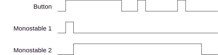
The Resume button needs more sophisticated debounce circuitry due to the following scenario: when multiple HLT instructions are separated by a relatively small number of other instructions, a pulse on the order of milliseconds (like the reset and pulse debouncers) will be far too long at high clock frequencies. The resume signal will still be high when a second (or third, fourth, ...) HLT instruction is encountered, causing control flow to simply skip over these instructions. To remedy this situation, a debouncing circuit is required that first produces a pulse equal in width to the clock pulses (Figure 19), followed by a guaranteed period where the signal is low, even when the button bounces after the pulse. This is achieved by creating a feedback loop between the two monostable multivibrators present on the 74LS123. The first one will produce a 200ns pulse on the rising edge of the button. This pulse is sent to the reset of the register that holds the HLT signal in order to clear it, but is also connected to the second monostable multivibrator. When the initial (short) pulse goes low, the second multivibrator generates a much longer pulse that is connected to the reset input of the first one, making sure it cannot be reactivated for some time.
To determine the RC values for the ’123, we aim for a cooldown period of around 1 second. The diagram from the datasheet is suitable for only short (up to 10 s) pulses, so instead we use the formula from the same page to find suitable values: Here, is measured in and is measured in . The result is the pulse width measured in ns. Setting and (both commonly available values for these components), the factor between brackets nearly vanishes to 1, yielding a pulse-width of
By selecting a 680K resistor and a 4.7 capacitor, a cooldown period of around 1 second is achieved. Figure 20 shows a timing diagram to illustrate this process in more detail.
Register Driver
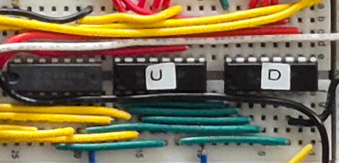
The register driver is responsible for driving the U and D inputs of the 74LS193 counting registers that are used to implement the D, DP, SP, IP and LS register modules. To increment the ’193, its D input needs to be held high while providing a low pulse to the U input. As explained in Section Register Driver, a centralized driver was used to limit the number of logic ICs necessary to drive the registers and the total number of control signals necessary.
Decoders
The driver module uses a pair of 3-to-8 decoders (74LS138): one to drive the U inputs and the other to drive the D inputs of the ’193. The ’138 takes 3 address bits (A, B and C) to select one of 8 outputs (Y0–Y7), which will be pulled low when selected (all other outputs remain high). Two gate inputs, G1 (active high) and G2 (active low), are used to enable the outputs of the chip; the selected output is activated (pulled low) only when both gates are active. This is very convenient given the fact that the 74LS193 needs a low pulse to increment or decrement its value:
The register-select signals RS0, RS1 and RS2 are connected to A, B, and C to select the required output.
The INC and DEC signals are connected through inverters to the G2 gate.
The module clock signal is connected to G1: when pulsed, the selected output will produce a pulse that is effectively an inverted clock pulse (high-low-high), which is exactly what the ’193 expects.
DP Register
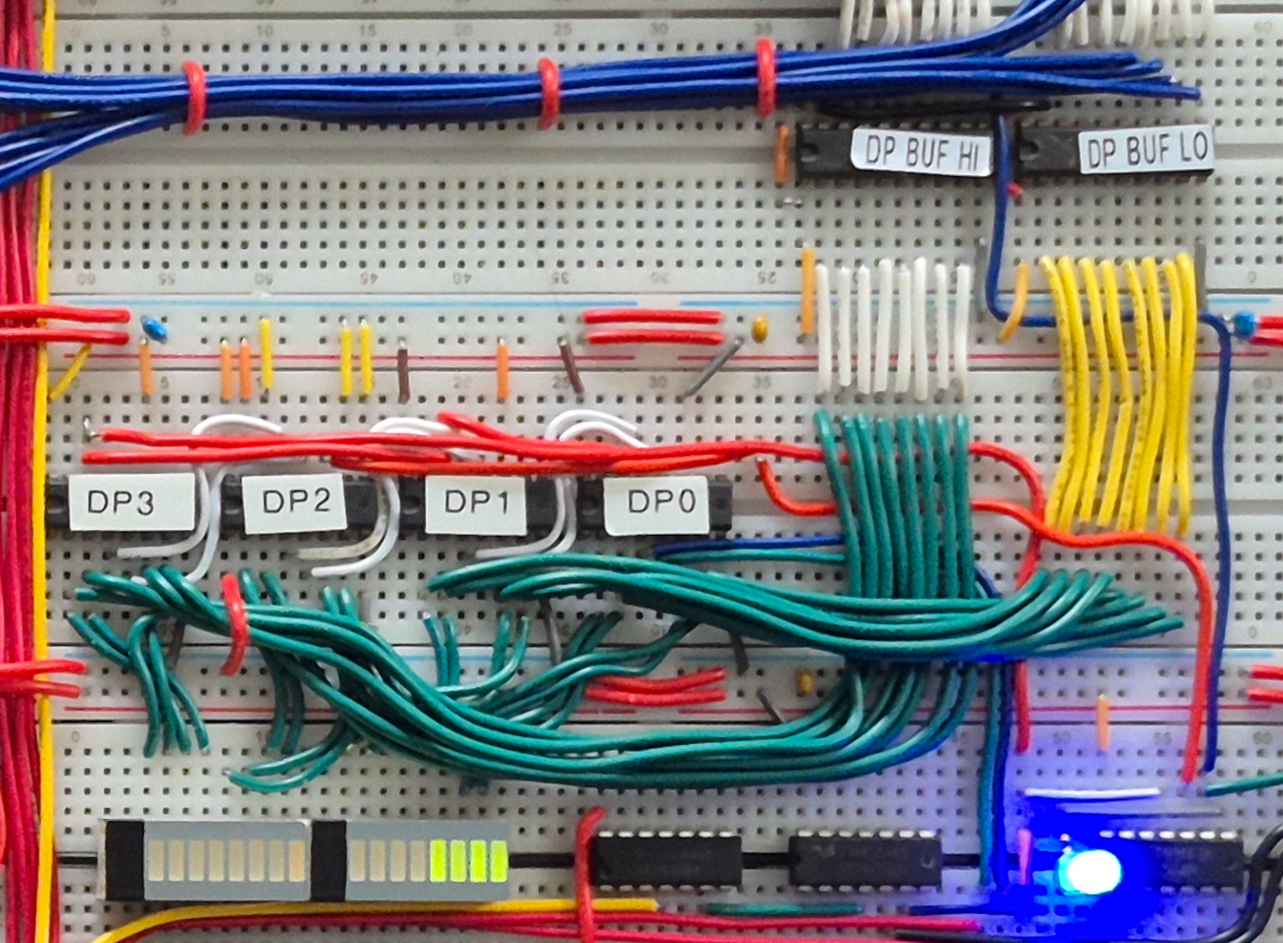
The DP Register Module is the module that is responsible for managing the data pointer; it contains a 16-bit value that is connected to the address bus of the RAM and points to the memory cell currently pointed to by the BF pointer. The value is stored across four 74LS193 binary counters that are chained together (each holding 4 bits), making it possible to address a total of different memory cells. The DP is connected to the register driver at address 2 (0b010, see Table 1) and as such can be incremented or decremented when the program hits a > or <, respectively. The outputs of each ’193 are connected to the address bus through a pair of tristate buffers (74LS245) to prevent bus contention with the stack pointer; see below (Enabling Output) for more information on the enable signal.
Reset Vector
Since the data section in RAM starts at 0x0100 (0x0000 through 0x00FF are reserved for the stack), this is the value that the register should start at right after booting up the system (all other registers start out with an initial value of zero). To achieve this, the global reset line of the system is connected to the reset pin of the ’193s corresponding to nibbles 0, 1 and 3, but to the load pin of nibble 2, whose inputs have been hardcoded to 0b0001 (0x1). This register is also special in the sense that it is the only register that needs to reset at runtime (through the CLR_DP signal), without resetting any of the other modules. After all, after initializing its memory to 0 by looping through (part of) its addressable space, the DP needs to be brought home to the start of the data section before the main program starts (see also Section Initialization and Bootloading). The global RESET signal is therefore ORed with the CLR_DP signal before going to the reset (and load) pins of the ICs.
Enabling Output
Perhaps somewhat confusingly, the schematic (see below) shows that the SP_EN signal is used to enable the buffers. Because the DP shares the address bus with only the stack pointer (SP)—and their outputs should be mutually exclusive—the same signal can be used to enable and disable their respective buffers: when the stack pointer is enabled, the data pointer should be disabled and vice versa. Given that the output enable pin of the 74LS245 is active low, the SP_EN signal can be fed directly into the enable pin of the DP buffers. On the side of the SP, the same signal goes through an inverter before going into the enable pin of its respective buffer. By default, when the SP is not enabled, the DP will provide its address to RAM. The address bus will therefore never be left floating, which has the nice side effect of always being able to visually see the current value in RAM by the LEDs connected to its outputs.
D Register
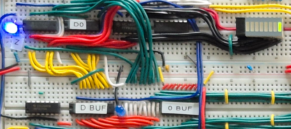
The data register (D) holds (a copy of) the value in memory currently pointed to by the data pointer (DP). In the computer, it is located in the top left corner. Like the DP, it is implemented using 74LS193 counting registers and driven by the register driver described in Section Register Driver at address 1 (001, see Table 1). Since the data is only 8 bits in size, no more than two ’193 chips have to be chained together to create the 8-bit register.
Enabling Output
The outputs of the ’193s are buffered by a single 8-bit tristate buffer (74LS245) before being connected to the data bus. Because the data bus is 16 bits wide (necessary to store IP values on the stack), the high byte is set explicitly to 0 when D is enabled by a second buffer that always outputs zeros. Storing nonzero values in the high byte of the data section would not have any consequences for the computation, but would be visually confusing. The buffers are set to output mode only (even though the register is able to read from the bus as well) because the ’193 chips have separate pins for incoming and outgoing data. The incoming data is read from the bus directly without needing to go through a buffer.
Z-Flag
This module also produces the Z-flag, indicating that it is currently containing the value 0. This is achieved by connecting its outputs through an 8-input NOR gate (MC14078B). The output of this gate is then connected to the FB flag register where it can be latched in by the CU in order to determine the next course of action.
Loading Data
Because the ’193 loads asynchronously, the clock has to be gated with the LD_D signal through a NAND gate in order to load synchronously with the clock when the LD_D signal is high (the load-pin on the ’193 is active low). The necessity of a NAND gate meant it was easier to also implement any inverters needed in the circuit in terms of NAND gates.
IP Register
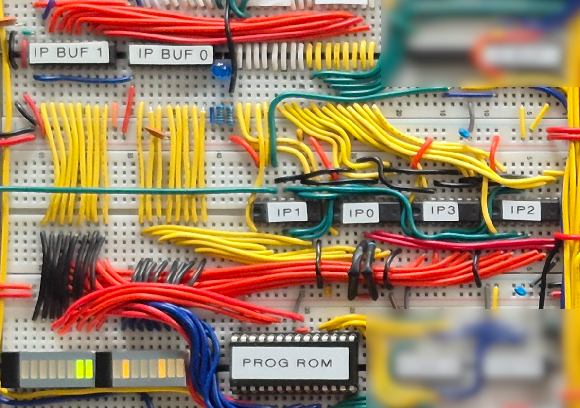
The instruction pointer register holds a 16-bit value representing the address of an instruction in the program-ROM (implemented using an EEPROM chip (AT28C64B)). The size of the available address space in program-memory is instructions, so the two uppermost bits (bits 14 and 15) of the IP are left unused.
Forbidden Decrement
The IP, like the D and DP registers, is driven by the Register Driver at address 4 (100), but should in principle never be decremented; it either moves to the right (next instruction) or jumps back by loading a value from the data bus. Its inability to move left (decrement) is not enforced by the hardware itself, but should be taken care of by the microcode implementation.
Reading and Writing Data
The IP is connected to the data bus through two tristate buffers (74LS245) to avoid bus contention with the D register and IO module. It is connected to this bus in order to write its value to the stack when a loop is entered. When exiting from a loop, a value is read back into the register through a direct connection to this bus (without going through a buffer). Because loading is done asynchronously on the ’193, the load signal is NAND’ed with the clock to make loading synchronous again.
SP Register
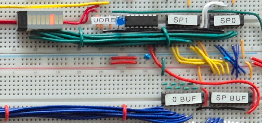
The stack pointer (SP) holds an 8-bit value in the range 0x00 - 0xFF, which corresponds to addresses within the stack space of RAM, where IP values can be stored and loaded from when the system sees the [ and ] loop instructions. When a loop is entered, the SP first increments its value and the IP register then stores its value on the stack at the resulting address. The SP is now ready for the next value to be stored on the stack when a nested loop is encountered. It is therefore implemented using the 74LS193 binary counter and connected to the register driver at address 3 (011). The SP module is connected to the same RAM address bus as the DP, which means it should go through a tristate buffer to avoid bus contention. As mentioned before (DP Register), the SP buffer shares its enable line (though inverted) with the DP. A second buffer that, when enabled, only outputs zeros on the address bus is used to make sure that only the stack is addressed by the SP and no accidental reads or writes happen in the data section.
LS Register
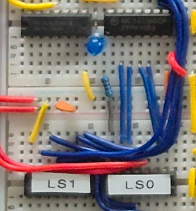
The Loop Skip Register (LS) is used to produce the loop skip flag (S, see Loop Skip Register (LS)). It is implemented using two 74LS193 binary counters and is connected to the register driver at address 5 (101). Like the Z-flag, the S-flag is produced by sending the outputs of the binary counters through an 8-input NOR gate, the output of which is then inverted and connected to the FB flag register. When any of these bits are high, the S-flag will be raised, indicating that the computer is in the process of skipping the current loop.
Flag Registers
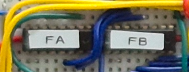
There are two stages of flag-buffering; the first stage is the FA register (in which the A and V-flags are stored) and the second the FB register (in which all flags except K are latched when the instruction is loaded). Both of these registers have been implemented using a 74LS173 4-bit register.
FA
The A and V flags are stored in FA by the CU whenever the value in D is changed (V) or whenever the pointer changes its position (A). This can happen mid-instruction without changing the address on the microcode EEPROMs.
FB
At each cycle 0, the A and V-flags are loaded from FA into FB, together with S and Z coming from the LS and D registers respectively. Since this always happens in conjunction with loading the instruction from program ROM into the instruction register (see Control Unit), the control signal has been named LD_FBI. The flags in the FB register will (mostly) remain constant during the execution of an opcode.
RAM
Capacity
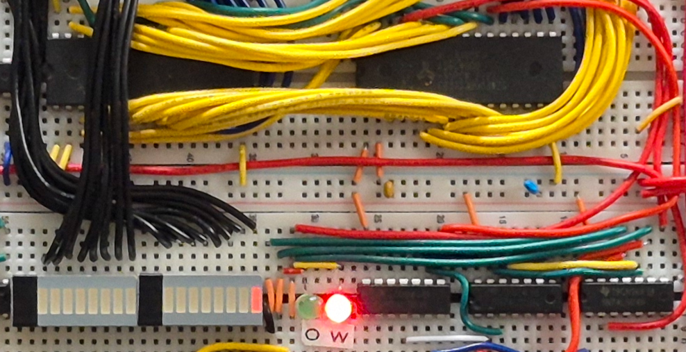
The RAM module is mainly used to store the 8-bit data of the BF memory tape. However, its secondary purpose is to also store the instruction pointer values when loops are handled, which are 16 bits in size. Therefore, the RAM module contains two 512K 8-bit SRAM chips (AS6C4008). Although each chip physically contains 512 KiB, the 16-bit address bus exposes only 65,536 paired addresses, for a total of 64K accessible 16-bit memory cells. When the data register’s output is enabled, its value will be stored in the lower byte of RAM (chip 0); the high byte (chip 1) is filled with zeros. The second chip is therefore only used to store the high byte of the IP. Since the stack can only store up to 256 values (in the address range 0x0000–0x00FF), the remainder of the accessible capacity of the RAM chip storing the high byte will never be used. Though this might look wasteful, it was preferred over the alternative of using two sequential bytes on the same chip to store the low and high bytes separately. This would have introduced more complexity in the surrounding logic and would have led to multiple cycles for reading from/writing to the stack, negatively impacting performance.
Buffering
The AS6C4008 already provides a Chip Enable input which is supposed to be used when the data is connected to a data bus. When this input is inactive, its outputs are in a high-impedance state to avoid bus contention with other devices. However, in this project we need the data currently pointed to to be visible on an array of LEDs, which means that the chip should be enabled basically at all times (except when writing to it). Additional logic is used in conjunction with a pair of 74LS245 tristate buffers to intercept the outputs before making them available on the bus through the buffers. The truth table for this logic is shown in Table 3. The LEDs are not shown in the schematic, but have been connected directly to the data lines of the RAM in this configuration.
| Module | RAM | Buffers | ||||||
| OE | WE | CLK | CE# | OE# | WE# | AB | EN | |
| 0 | 0 | 0 | 0 | 0 | 1 | 1 | 0 | Show data, but do not send to the bus. |
| 0 | 0 | 1 | 0 | 0 | 1 | 1 | 0 | Show data, but do not send to the bus. |
| 0 | 1 | 0 | 1 | 1 | 0 | 0 | 1 | Prepare to load value from the bus. |
| 0 | 1 | 1 | 0 | 1 | 0 | 0 | 1 | Load value from the bus. |
| 1 | 0 | 0 | 0 | 0 | 1 | 1 | 1 | Send value to the bus. |
| 1 | 0 | 1 | 0 | 0 | 1 | 1 | 1 | Send value to the bus. |
| 1 | 1 | 0 | 1 | 1 | 0 | 0 | 0 | Should not happen (chip disabled). |
| 1 | 1 | 1 | 1 | 1 | 0 | 0 | 0 | Should not happen (chip disabled). |
Control Unit
Overview
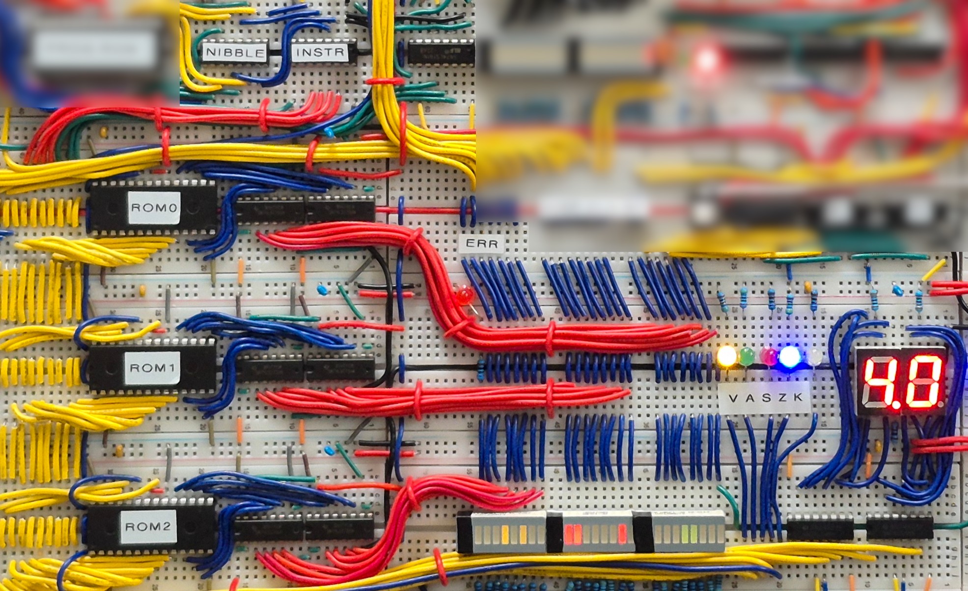
The control unit is responsible for sending the appropriate control signals to each of the modules. The general idea is that the current instruction pointed to by the IP (4 bits), together with the state flags (another 5 bits: K, A, V, S and Z) and the cycle count (3 bits), combines to form a 12-bit address into a set of three EEPROM chips (AT28C64B), each of which contains part of the signal configuration corresponding to the current state of the system. When clocked by the decoder clock (D_CLK), the values currently at this address are loaded into six 74LS173 registers (two per EEPROM) and asserted onto their respective modules, which will act upon them on the next pulse of the M_CLK signal.
Address Layout
Based on the physical layout of the board, the following configuration was used to construct an address into the EEPROMs.
| Address Bits | ||
|---|---|---|
| 0-2 | Cycle count | ( - ) |
| 3-6 | Instruction | ( - ) |
| 7-11 | Flags | ( - ) |
| 12 | Unused |
Generating and Programming Microcode
The three EEPROMs have been programmed using a custom-built EEPROM programmer based around an Arduino Nano, combined with a Python script (bflash.py) that is able to send a binary image to the Nano over a serial connection. The images that store the microcode tables have been generated by Mugen (see Microcode Compiler (Mugen)), a utility developed to make the microcode programming more maintainable. Mugen generates the images from a specification file. The full Mugen specification for Synapse-191 is shown in Appendix Mugen Specification. This is a direct representation of the microcode shown in Table 15 (Appendix Microcode Table).
Instruction Nibbles
The actual BF program is stored in another 8K EEPROM chip (AT28C64) and is addressed by the instruction pointer as mentioned before. Since each BF instruction only needs 4 bits to be encoded (there are fewer than 16 different opcodes), we can store up to 16K instructions in the chip by packing 2 consecutive instructions together in a single byte (handled by the assembler, bfasm). Rather than using bit 0 from the IP directly as address bit 0 on the EEPROM, it is used as the data select signal to a 74LS157 multiplexer. This multiplexer takes 1 select bit and two sets of 4 data bits. Depending on the value of the select bit, one of the sets of 4-bit data is sent to its outputs. This allows us to select either the low or high nibble of the data in the EEPROM, effectively doubling the number of instructions that can be stored and retrieved.
Instruction Register
The selected nibble is loaded into the instruction register (I) at the same time as the V, A, S and Z flags are loaded into the FB register. For this reason, both the FB and I registers can operate on the same control signal: LD_FBI. The I register is implemented using the 74LS161, which is actually a counting register, because at the time there was no ’173 available anymore and these chips are functionally almost identical when counting is disabled on the ’161. Initially, the outputs of the multiplexer (’157) were directly connected to the address lines of the microcode EEPROMs, but when it turned out that this could cause instabilities on some rare occasions, the I register was added to buffer the instruction for the entire duration of the opcode execution.
Cycle Counter
The cycle counter is implemented by a 74LS161 binary counter that simply increments on every M_CLK signal and sends its outputs (bits 0–2) to address lines 0–2 of the microcode EEPROM chips. It is reset when it receives the CR signal (which becomes active after an instruction has completed).
Early Segmented Implementation
In the initial implementation of the CU, the entire microcode lookup-table was implemented in a single EEPROM chip. Two additional address bits, the segment bits, were included to address at most 4 different sections of the ROM (at the time, the K-flag did not exist yet, leaving the final two address bits 11 and 12 free to use for this purpose). Each section contained an 8-bit control word, such that rather than latching the entire 24-bit control word in a single clock, the logic was designed to access each of the 3 control words sequentially and latch them one by one before clocking the modules. This design choice was made back then because of the low availability of the AT28C64B chip; only two of these chips were acquired, one for storing the program and the other for storing the microcode. While chip-efficient, this approach requires 3 times as many clock cycles per instruction and was abandoned as soon as we got our hands on more EEPROM chips. Moreover, in our current implementation only one address bit (12) is free to use due to the K-flag being added in a later stage of the build, leaving no more room for segmentation even if we wanted to. Figure 63 in Appendix Flashback shows the system at a point in time where the segmented CU was still present.
IO Module
Features
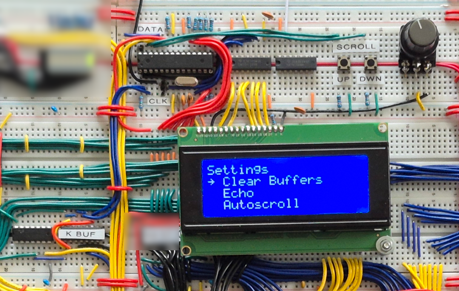
The IO system is handled by an ATmega328P microprocessor, commonly found in the Arduino Uno. It has five main functions:
Supply the program slot index to the system bus at boot.
Drive the screen and display contents from the bus when instructed to by the
EN_OUTsignal.Handle keyboard input and provide input data to the bus when instructed to by the
EN_INsignal.Provide a random number to the bus when both signals are supplied (implementing the Random Brainfuck Extension).
Supply a menu system to alter its settings using two buttons.
Buttons and Menu
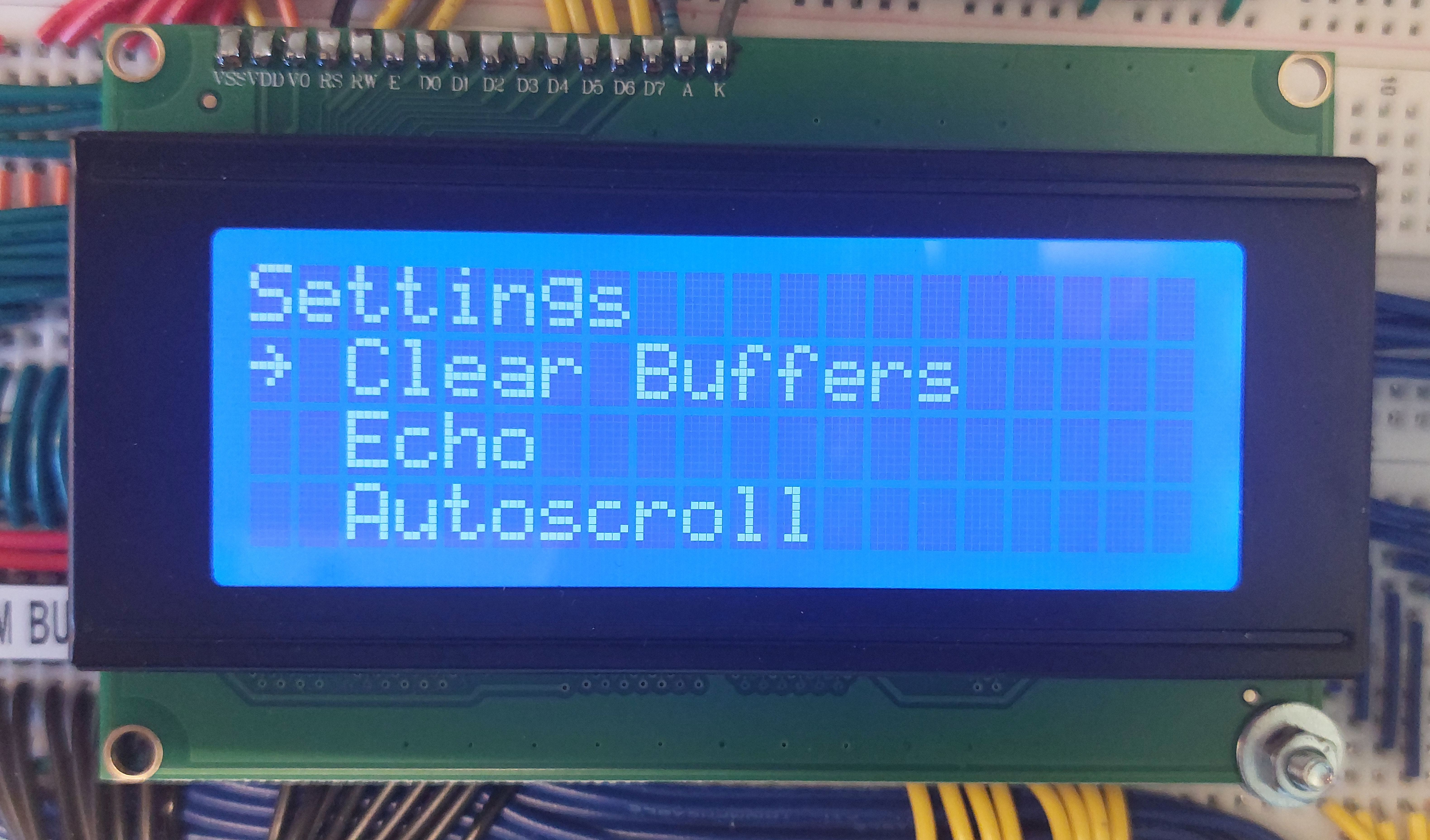
Two buttons are provided to interact with this system. They can be used to scroll the screen or to access and navigate a menu (Figure 31). This menu lets the user do the following:
Select the program slot that is loaded by the system on reset.
Clear the screen and keyboard buffer.
Change the display-mode. By default, incoming data is interpreted as ASCII characters. When it should be displayed as raw numerical values (either in base 10 or 16), this option can be selected from the menu. When in either of these numerical modes, a delimiter character can be selected to separate bytes visually.
Set autoscrolling on/off. By default, the screen will scroll its contents when they overflow to always keep the most recent data in view. When new data is displayed, the screen is always scrolled to display this data. Setting autoscroll to ‘off’ will disable these features.
Echo on/off. When running an interactive program that requires keyboard input, the user probably wants to see what is being typed. This is the default behavior (echo on). If for some reason the keypresses should not be displayed, this option can be disabled.
Set the input-mode. By default, the IO module will wait for the input-buffer to contain a value before putting anything on the bus and notifying the CU through the K-flag (buffered input-mode). However, an alternative mode (immediate) can be selected, in which case the IO module will put a zero on the bus when the buffer is empty and set the K-flag regardless. This can be helpful if programs require real-time inputs (e.g. for simple games).
Set the RNG seed. For programs that use the Random Number Generator as an input device, the seed can be set through this option. Since the same seed will produce the same sequence of numbers, this option can be used to control the randomness of the application. A ‘true’ random seed can normally be emulated by seeding the generator with the reading of a floating analog input, for example, but sadly no free analog inputs were left available on the MCU.
Reset to default settings. Whenever settings have been changed, the new settings will be saved to the persistent EEPROM memory of the MCU and loaded back on startup to make the settings persist when the MCU is powered down. This option allows you to revert all changes and load the default settings back in.
System Interactions
K-Flag
The K-flag acts as an asynchronous barrier between the IO module and the rest of the system. It can be set by the module and is reset by the main system; this allows for synchronized communication between two asynchronous systems. It is implemented as a dual D flip-flop (74LS74), of which the first flip-flop is set asynchronously (w.r.t. the main system) by the IO module. The output of this flip-flop is then latched synchronously into the second flip-flop on every system clock edge (M_CLK), the output of which is fed into the CU together with the other flags. The CLR_K signal emitted by the CU will reset both flip-flops on the next M_CLK pulse, indicating to the module that some transaction has been completed. The flag is used during boot (to communicate the program slot index), during the OUT instruction (to indicate that the output byte has been received) and during the IN instruction (to indicate that the input byte has been received). Because of space limitations, the logic necessary to clear the flip-flops synchronously (the ’74 has asynchronous clear lines, active low) was implemented in terms of NOR gates, requiring only a single 74LS02 quad NOR chip. Setting R = RESET, K = CLR_K and C = M_CLK, the logic required to drive the clear lines of the flip-flops (Q) can be written as The output Q is driven low when either the RESET line goes high or the CLR_K is asserted together with the clock. This can be rewritten in terms of NOR-operations (using to denote the NOR operator) as and finally, replacing the NOT-operators with NOR-operators as for a total of 4 NOR gates.
Bootloading
The first transaction between the system and the IO module happens at boot: the IO module is expected to put the index of the program (selected by the user through the menu) onto the data bus. However, when the system is reset, it will first initialize its memory. This process involves data transfers over the data bus, so the IO module should wait for a signal from the system to indicate that the initialization is completed and the data bus can be used safely. To achieve this, the IO module enables the K-flag and waits for it to be set low by the system. Next, it will write the program index to the bus, again setting K to indicate that this value is ready. The system will then read this value from the bus and acknowledge the transfer by resetting K once again. Once the IO module sees K going low again, it will disable its outputs and go to its normal operation, listening for input and output commands.
Output
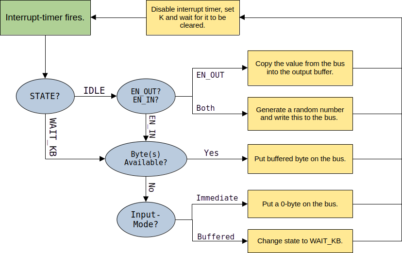
An interrupt attached to a timer fires at a set interval. When the system is in its IDLE state, it will check the EN_IN and EN_OUT lines to determine if it should initiate a read or write sequence to the data bus. When EN_OUT is found to be high, it will copy the byte currently present on the bus into its screen buffer, set the K-flag and wait for the CPU to reset K before waiting for the next instruction. When K is seen to go low, the handshake has been completed and the module returns to its IDLE state (see Figure 32).
Input
If the EN_IN signal is found to be asserted, the system has two possible courses of action, depending on the input mode currently set by the user (through the on-screen settings menu). In the (default) buffered mode, the system will change its state to WAIT_KB and wait for a byte to become available in the keyboard buffer. As soon as it does, it will provide this value onto the bus and notify the CU by setting the K-flag. It then waits for K to go low again, confirming that the CU has taken the value from the bus and that the module should release the bus again. In immediate mode, all zeros will be written to the bus and the K-flag is set immediately even when the keyboard buffer is still empty. If, in addition to EN_IN, EN_OUT is asserted as well, a random byte is put onto the bus (see Figure 32).
Shift Register
A shift register (74HC595) had to be used to decrease the number of pins on the ATmega328P necessary to drive the LCD screen. Every IO pin has been used, so the shift register proved invaluable for this application.
LCD Screen
The software was written in such a way that most common LCD character screens (compatible with the Hitachi HD44780 driver) will be handled appropriately. Both a 16x2 and a 20x4 display have successfully been installed in the computer. A modified version of the LiquidCrystal_74HC595 library was used to implement the LCD driver.
Keyboard
The IO module can only handle input from PS/2 compatible keyboards. A modified version of the PS2Keyboard library was used to implement the keyboard driver.
IO Module Firmware
To ensure minimal latency and efficient CPU–peripheral communication, several low-level optimizations were applied to both the interrupt routine and the main execution loop of the module’s firmware.
Interrupts
To make sure the module remains responsive during operation, regardless of I/O throughput, its input signals (EN_IN and EN_OUT) are checked at regular intervals, triggered by a timer interrupt. This timer fires at a rate of 200 Hz and triggers a highly optimized, low-cost interrupt service routine (ISR) that inspects the input signals and performs the corresponding action. Even when the ISR triggers at only 200 Hz, this will feel close to instantaneous to the user operating the computer. This leaves plenty of time for the microcontroller to drive the screen, handle the button input and manage the menu system. When the ISR is triggered by the timer and it is determined that some action needs to be taken, the K-flag is set to indicate to the external system that the action has been completed (see below). When K is finally cleared, the microcontroller needs to respond immediately because the system expects it to release control of the bus immediately after K is cleared (e.g. after responding to the EN_IN command). Therefore, the same 200 Hz interrupt cannot be used for checking K. Instead, the timer is stopped before checking K and a second ISR is attached to the falling edge of K. This ISR will trigger immediately when K goes low, allowing the microcontroller to respond quickly and set its data pins back to a high-impedance state (pinMode(X, INPUT) in Arduino nomenclature). It will then re-enable the timer to go back into normal operation. The C++ code that represents the state machine previously shown in Figure 32 is shown in Listing 16 (Appendix IO Module ISR).
Ring Buffers
Overview
The IO module employs a set of custom ring buffers that provide high-speed, non-blocking data transfers between the asynchronous microcontroller firmware and the synchronous TTL-based CPU. The ring buffer (or circular buffer) is a fixed-size, first-in-first-out (FIFO) data structure that uses two indices, commonly called the head and tail. The head marks the position where the next incoming element will be written, while the tail indicates the position of the next element to be read. When either index reaches the end of the buffer, it wraps around to the beginning, forming a logical ring in memory. This structure eliminates the need for memory allocation or data shifting, providing constant-time access for both enqueue and dequeue operations. See Figure 33.
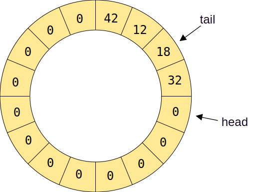
tail) will be returned on the next query. Data entering the ring buffer will be stored at the cell pointed to by head. The value 42 is the first value to be overwritten when the head pointer wraps around to the top of the buffer.In the Synapse-191 I/O module, one ring buffer is dedicated to temporarily storing incoming data (bytes coming from the CPU that need to be written to the LCD screen), the screen-buffer, and another is used for outgoing data (keyboard input that needs to be put on the data bus), the keyboard-buffer. The main loop periodically flushes the screen-buffer to the display and refills the keyboard-buffer with new data when it arrives. Meanwhile, the interrupt service routine (ISR) accesses these buffers asynchronously to satisfy CPU read and write requests. Since all the heavy lifting (interpreting incoming data, managing the LCD screen, decoding keyboard scan-codes) is done in the main-loop, the ISR is kept very compact.
Optimizations
The ring buffer is implemented as a templated C++ class, parameterized by buffer size and value type. Several compile-time and runtime techniques were employed to maximize performance and memory efficiency. A combination of compile-time specialization and minimal arithmetic overhead allows the ring buffers to perform low-overhead enqueue and dequeue operations, which is essential for keeping up with the ‘high’ frequency external system clock of the Synapse-191 CPU.
Index Type Specialization: The index type (data type used to store the
headandtailindices) is selected automatically at compile time using template metaprogramming. For small buffers, 8-bit indices are used instead of 16- or 32-bit counters, reducing instruction count and register usage and thus ensuring the fastest possible integer operations on our 8-bit MCU.Integer Wrapping Optimization: For buffers that are exactly as big as the maximum number representable by some type, that type is used to index the buffers as per the logic above. For example, a 256-byte buffer can be indexed fully using an 8-bit type like
unsigned char. A value of 255 represented by this type will automatically wrap around when incremented, rendering any additional modular arithmetic to wrap around to the start of the buffer unnecessary.Power-of-Two Optimization: When the buffer size does not match the condition above, but is a power of two, the modulo operation used for index wrapping is replaced with a simple bitwise
ANDoperation:i = (i + 1) & (N - 1). This reduces the naive modulo operation from multiple CPU cycles to a single instruction.
Volatile Access and Memory Barriers
The head, tail, and data array are declared volatile so that their accesses are emitted rather than cached or optimized away across the ISR and main loop. Additionally, an inline assembly memory barrier prevents the compiler from reordering memory accesses across the barrier, ensuring that writes to the buffer occur before the corresponding index is updated.
Direct Port Access
The ISR itself is further optimized using direct port manipulation. Instead of relying on Arduino’s digitalRead(), digitalWrite() and pinMode() functions, which incur significant overhead, the firmware performs raw register accesses (PORTX for writing, PINX for reading and DDRX for changing modes) through custom inline functions. This facilitates faster control over timing-sensitive pins.
Compile-time Menu Structure
Finally, the on-screen configuration interface uses a statically defined menu tree that is fully constructed at compile time using template metaprogramming techniques. This eliminates dynamic memory allocation and object initialization overhead during runtime, minimizing both execution latency and memory footprint. Together, these optimizations produce a maintainable, fast and memory-efficient IO subsystem capable of operating reliably at high CPU-core clock speeds.
using Menu = MainMenu <
  SelectSlot<
    SlotSelecter<0, N_SLOTS - 1>
  >,
  Clear,
  Echo<
    EchoOn,
    EchoOff
  >,
  Autoscroll<
    AutoscrollOn,
    AutoscrollOff
  >,
  DisplayMode<
    TextMode,
    DecMode <
      CommaDelim,
      SemiDelim,
      BarDelim,
      SpaceDelim
    >,
    HexMode<
      CommaDelim,
      SemiDelim,
      BarDelim,
      SpaceDelim
    >
  >,
  InputMode<
    BufferedInput,
    ImmediateInput
  >,
  SetRNGSeed<
    SeedSelecter<RNG_MIN_SEED, RNG_MAX_SEED>
  >,
  Defaults,
  Exit
>;