Conclusion
This project set out as a “What if?” for which expectations were deliberately kept low. A functional system was the goal; not a fast one. We had no idea what kinds of speeds we could expect, how stable the system would be and frankly whether we would even end up with anything functional. The only goal was simply to get something going. Given those goals, this project has certainly delivered to an unexpected extent.
Building Synapse-191 has been a tremendously powerful learning experience. Above all, the joy of seeing months of tedious work, planning and debugging culminate into a working system is unparalleled. The system’s specifications themselves never prevented any of the tested BF programs from running; it has never run low on memory, has a large enough program-ROM to store BF code and has plenty of stack-space to run even computationally demanding programs. Features like the IO system, being able to store multiple programs to select from, single-stepping and easy control of the clock make it an enjoyable process to operate the computer. Moreover, with the toolchain developed to a mature state, adding features through modification of the firmware and microcode was relatively straightforward and thoroughly rewarding to do.
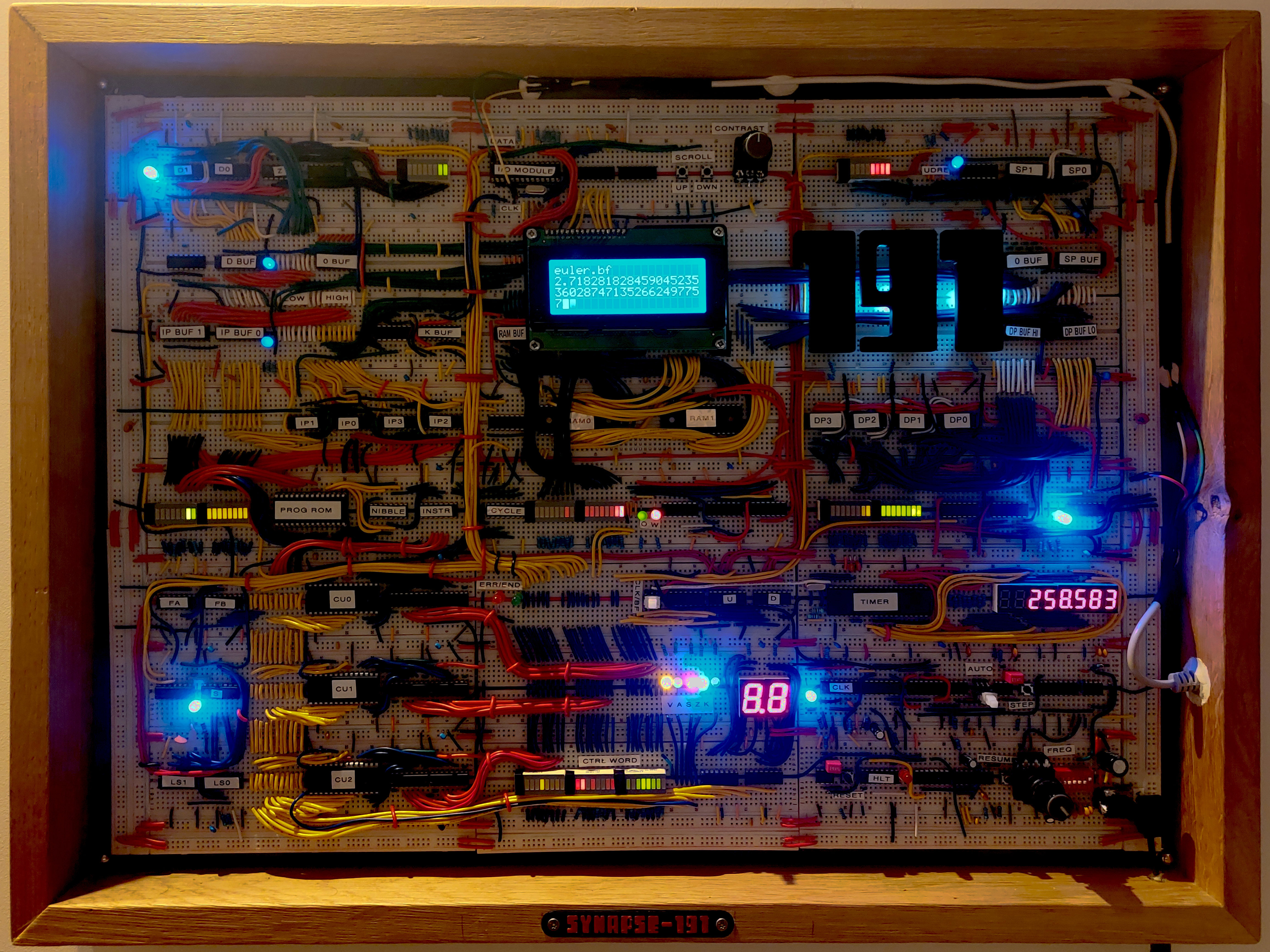
The system has at the time of writing been framed and hung from a wall. External ports have been added to the frame such that even when hanging, it can still easily be plugged in and controlled using the keyboard. Some 3D-printed parts have been added for visual effects, but no further extensions will be added to the system as-is. There are currently no plans for future development of a next generation (e.g. on a PCB), because what’s the point? Then again, what was the point, ever?
Final Thoughts
Virtual Registers
A big limitation of using the register driver as a centralized system to increment or decrement each register is the fact that only one register can be addressed per clock cycle. Having two addresses on the register driver still unconnected (addresses 110 and 111), their corresponding outputs could be connected to multiple registers that commonly need to increment together. For example, address 110 (bits RS2 and RS1) would then correspond to the virtual register D/IP. The corresponding U and D output signals would then be connected (through OR gates) to the counting inputs of both the D and IP register. Addressing this virtual register would then allow for incrementing or decrementing these registers simultaneously, which saves a clock cycle in the PLUS instruction. The MINUS instruction does not benefit from this trick, since we can’t both decrement D and increment IP at the same time. The same could be done for DP and IP, saving a clock cycle in the RIGHT instruction.
Some preliminary tests on the programs from the test suite (using again the modified interpreter to acquire statistics) show that 30 to 40% of all instructions executed at runtime are either + or >. Based on this data, we can set some boundaries on the estimated increase in performance when the aforementioned virtual registers (D/IP and DP/IP) would be implemented. Assuming 3.5 cycles per instruction under current circumstances (see Chapter Runtime Results), this number would be reduced by 1 cycle in 40% of all instructions (in the optimal case), leading to a decrease of cycles per instruction on average, or about a 10% performance increase.
No Register Driver
Taking the considerations above even further, one could argue that the system would do even better with no register driver at all. Granted, this would have required four additional control lines (5 INC + 4 DEC for a total of 9 versus 1 INC + 1 DEC + 3 RS-bits) and would have required each register to implement logic that properly drives the U and D inputs of the ’193, but it is still worth considering what kind of performance improvement could be expected. As before, the gathered statistics allow us to estimate the fraction of instructions that would benefit from driving the registers in parallel, allowing for multiple INC and DEC instructions to execute simultaneously. Given the fact that we could even issue an INC and another DEC together (which wouldn’t have been possible with the virtual register), the +, -, < and > commands would all be improved by one cycle. These commands make up 70 to 80% of all instructions executed at runtime. A similar calculation then shows that the average number of cycles per instruction could drop by at least 0.7, all the way down to 2.8 cycles per instruction for a performance increase of 20%. However, since there currently are no spare control lines available, this would have required adding a fourth EEPROM to extend the control word beyond 24 bits. The system’s layout was frozen long before this consideration even came to mind, rendering this idea next to impossible to implement on the current version of the system without requiring a complete teardown.
Designing a PCB
Even though the system appears to run very stably at the time of writing, it is still very vulnerable given that it relies on springy connections that could oxidize or lose their tension over time. The durable approach would be to design a PCB with proper voltage and ground planes, stable traces between ICs and durable soldered connections. If this direction is ever going to be pursued, most LEDs would probably be removed to minimize the PCB’s footprint. We would also have to consider how the program ROM can be inserted and removed easily; maybe even using ROM on an expansion card like the NES of the old days. For maximal modularity, the IO module could be implemented as an expansion card; different implementations (perhaps even using graphics or sound instead of ASCII characters as their output mode) could easily be swapped in and out.
Going Full 16-bit
In Section RAM it was mentioned that the vast majority of memory cells in the second SRAM chip are left unused. Only the high byte of the IP values is stored in this chip when the IP is pushed to the stack on entering a loop, for a maximum of 256 bytes stored on a 512 KiB memory chip (of which 64 KiB is addressable through the 16-bit address bus); none of the other accessible cells are ever used. Since the data bus is already 16 bits wide, it would have been fairly easy to make the D register a 16-bit value as well. This would allow for BF programs that assume 16-bit data cells. Even though this was briefly considered in the early stages of the project, we chose not to go through with it because a) it is not canonical BF and b) we did not want to make the system more complex than necessary at the time (we would effectively need a 16-input NOR gate, requiring two more ICs on top of the two additional register ICs). In hindsight, this would have been a nice (and pretty achievable) feature to have.
Using the ’191
The 74LS191 seems like the perfect candidate to implement the counting registers. It simply has a U/D input to select the counting direction, a count-enable input (CTEN) and is connected directly to the clock. This is exactly how the register modules behaved in early abstract designs of the system. The ’191 was never used for the simple reason that we never knew about its existence and ordered the ’193 instead; that was the first chip we encountered that could do the job. In hindsight—and purely by luck—the ’193 was indeed the better choice because of its ability to (asynchronously) clear its values; the ’191 has no clear input. This would have made it more difficult to implement clean reset functionality. Also, the number of control lines to the modules would not have been different (U/D + CTEN instead of U + D), so the need for a register driver would still be there.
Decoupling Capacitors
When resorting to the internet (websites, forums, AI chatbots) to gather tips on stability, all of them mention the same potential solution: place decoupling capacitors (100 nF) as close as possible to the VCC and GND pins of every IC. Even though many of these have been placed around the board across the power rails, near the ICs, ideally they would have to be placed right across the ICs’ power pins (often located diagonally opposite one another). We never observed any improvements from placing such capacitors anywhere, so—naively—we never sacrificed looks for potentially more stability (placing the capacitors across the ICs doesn’t look very good in my opinion). If we were to start over again (and we won’t), these capacitors would have to be integrated into the design, just to be sure.
Using AI
LLMs like ChatGPT have proven a valuable tool while designing and debugging the system. Let’s be clear: no LLMs have been used to generate the text of this document or even write a single line of supporting code in the toolchain. It was, however, a valuable brainstorming partner when trying to find subtle logic bugs in both software and hardware. It almost never got it right completely on the first try, but it almost always inspired new avenues to explore. This more often than not led to us identifying the problem eventually. Thinking out loud together with a partner will often lead to new insights and, believe it or not, it is hard to find (human) sparring partners on a specialized project like this one.
IO Module: Cheating?
Should using an MCU in the implementation of the IO module be considered cheating? We set out to implement a BF computer without using any programmable chips, so clearly we broke our own rule, right? No. The entire BF core was implemented true to our mission goals: all BF commands are handled by TTL, RAM and ROM chips. The IO Module should be considered an abstract external device; its inner workings are irrelevant to the BF core logic in the same way that the BF language does not specify how user input is acquired or how data is displayed when issuing the , and . commands. Modern monitors and other peripherals often contain embedded driver chips that handle communication protocols or, in the case of monitors, display settings; this is no different.
Higher Clock Speeds
Once all the instabilities faded even at higher clock speeds (after a proper implementation of the K-flag to act as a synchronization barrier between the CPU and the IO module), it should in principle be possible to push the clock far beyond its current limits. These limits have now been imposed by the choice of RC combinations on the 555 timer and can be pushed even higher. Other breadboard implementations of homebrew CPUs have reported stable clock speeds in the MHz range. The reason for not doing this is purely pragmatic. Enough time has been sunk into this project as it is and it needs to end somewhere, exposing a human limit rather than a technical one.